
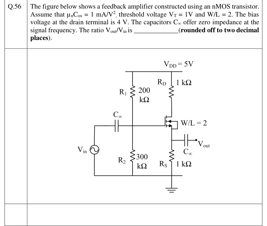
The figure below shows a feedback amplifier constructed using an nMOS transistor. Assume that , threshold voltage and . The bias voltage at the drain terminal is 4 V. The capacitors offer zero impedance at the signal frequency. The ratio is ________ (rounded off to two decimal places).
 Tap to open full size
Figure description
A single enhancement nMOS stage with supply V_DD = 5 V at the top rail. R_D = 1 kΩ connects V_DD to the drain. The gate is biased by a divider: R_1 = 200 kΩ from V_DD to the gate node and R_2 = 300 kΩ from the gate node to ground. A source V_in (sinusoidal symbol, lower terminal grounded) drives the gate node through a coupling capacitor C∞. The body (substrate) is tied to the source, shown by the arrow connected to the source terminal; the device is labelled W/L = 2. R_S = 1 kΩ connects the source to ground. The output V_out is taken from the source node through a second coupling capacitor C∞, with no load drawn. All grounds (V_in return, R_2, R_S) are common.