
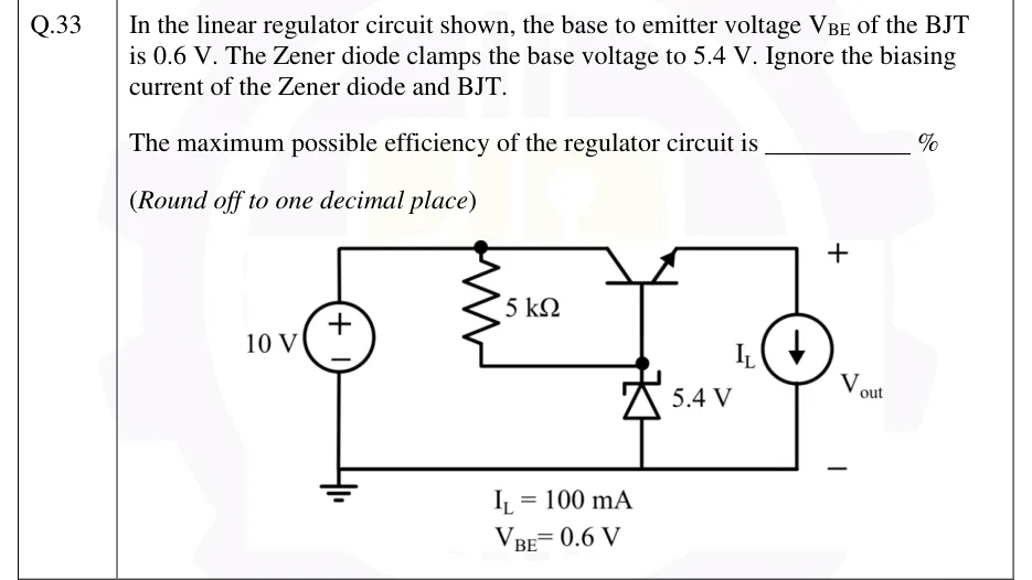
In the linear regulator circuit shown, the base to emitter voltage of the BJT is 0.6 V. The Zener diode clamps the base voltage to 5.4 V. Ignore the biasing current of the Zener diode and BJT.
The maximum possible efficiency of the regulator circuit is ________ %
(Round off to one decimal place)
(Figure data: , )
 Tap to open full size
Figure description
Series-pass (emitter-follower) linear regulator. A 10 V DC source (+ at top) has its negative terminal on the ground rail. The top rail from the source + goes to the collector of an NPN BJT (drawn horizontally: collector on the left, emitter on the right with the arrow pointing outward) and also to the top of a 5 kΩ resistor. The bottom of the 5 kΩ resistor connects to a node that goes up to the BJT base and down to the cathode of a Zener diode (anode to ground), labelled 5.4 V. The BJT emitter goes along the top right to an ideal DC current source I_L (arrow pointing down) whose lower terminal is on the ground rail; the output voltage V_out is taken across this current source, + at the top and − at the bottom. Labels under the circuit: I_L = 100 mA, V_BE = 0.6 V.