IAE Academy

GATE EC · EE · IN

Diode circuits

Clipping, clamping, rectifiers and regulators

Diode circuits use the diode's one-way conduction to shape waveforms and supply power: clippers limit a waveform, clampers shift it, rectifiers and filters turn ac into dc, multipliers raise the dc level, and Zener regulators hold it steady. Nearly every problem here comes down to one skill: decide which diodes are ON, replace each with the model the data calls for (ideal, constant-drop or piecewise-linear), and solve the linear circuit that remains. The rest is a short set of rectifier, filter and regulator results, and each one depends on stated conditions such as the diode model, a resistive or capacitive load, and which peak voltage V_m refers to.

25 previous-year questions · 25 solved · 7 practice questions

Diode models and the method of assumed states

A diode conducts easily when its anode is more positive than its cathode by about the cut-in voltage . When reverse-biased (below breakdown) it blocks, to a first approximation. Every circuit in this topic is solved by replacing each diode with a straight-line model that is valid in its present state. So the first decision in any question is which model the data asks for, and the second is which state each diode is in.

SHOCKLEY DIODE EQUATION

Exponential model of the junction below breakdown (series resistance neglected). = reverse saturation current, = ideality factor (1 to 2). mV at 300 K; these notes round it to 25 mV, and 26 mV is also common, so take the value the question gives. For , ; for , .

FORWARD VOLTAGE CHANGE WITH CURRENT

Valid when both currents are much larger than . With and mV, a tenfold change in current changes by 57.6 mV (about 60 mV with 26 mV).

DYNAMIC (SMALL-SIGNAL) RESISTANCE

Slope resistance at the dc operating current (valid for ), used when a small ac signal rides on a dc bias. With , mV and mA, .

TEMPERATURE DEPENDENCE (SILICON, NEAR ROOM TEMPERATURE)

At a fixed current the forward drop falls as temperature rises (figures between about and mV/°C are quoted, so use the value given). Problems often assume the reverse saturation current doubles for every 10 °C rise (about 7% per °C). This is a rule of thumb: some treatments give a faster rate for the ideal-junction , so if a question states a rate, use it.

Model

When ON (conducting)

When OFF

Use it when

Ideal

Short circuit: , any

Open circuit: any

The question says ideal, or the source voltages are far larger than 0.7 V

Constant-drop

Battery (0.7 V Si, about 0.3 V Ge),

Open circuit:

A cut-in or forward voltage is given and no resistance

Piecewise-linear

in series with :

Open circuit (or a reverse resistance if one is given)

A forward resistance is given

Exponential

is given, or a small-signal is needed

Method of assumed states

  1. Guess a state (ON or OFF) for every diode, usually from the direction in which the source pushes current.

  2. Replace each ON diode by its model (short, battery, or plus ) and each OFF diode by an open circuit.

  3. Solve the resulting linear circuit.

  4. Verify: every ON diode must carry from anode to cathode; every OFF diode must have ( for the ideal model).

  5. If a check fails, change that diode's state and solve again. With several diodes, change one at a time, starting with the most clearly violated.

  6. For a time-varying input, find the breakpoints: the input values at which a diode changes state ( and at the same time). Between breakpoints the circuit is linear, so the transfer characteristic against is a set of straight segments.

EXAM TIP

Use exactly the model the data implies. If the question says ideal, do not subtract 0.7 V; if it gives a cut-in voltage, do not ignore it. An answer worked with the wrong model is still a reasonable-looking number, so it will not look wrong.

EXAM TIP

Suppose two diodes connect one node to different voltages, or have different cut-in voltages. The diode that turns on first fixes the node voltage and can hold the other OFF. Check this with assumed states rather than assuming both conduct.

Clippers (limiters)

A clipper passes the part of the input on one side of a reference level and removes the part beyond it, without changing the shape of the rest. In a series clipper the diode sits between the input and the load; with the output taken across alone, the output is zero whenever the diode is OFF. In a shunt (parallel) clipper a series resistor feeds the output node, and the diode with its bias battery sits across the output. When the diode is OFF the output follows the input (exactly, when there is no load); when it is ON the output is pinned at the bias level plus or minus .

The reliable method is the transfer characteristic: find each breakpoint, draw against as straight segments, then read off the output for the given input waveform. The shunt-clipper results below assume no load (or ) and the constant-drop model; for an ideal diode, set . Sign convention for shunt clippers and clampers: is the signed potential, relative to ground, of the diode terminal that is not connected to the output node. A 3 V battery with its positive terminal to the diode and its negative terminal grounded gives V; the same battery reversed gives V.

UPPER-LEVEL SHUNT CLIPPER

Diode anode at the output node, cathode at potential . The diode conducts, and the output is flat, for .

LOWER-LEVEL SHUNT CLIPPER

Diode cathode at the output node, anode at potential . The diode conducts for . With the anode at V, for example, the output cannot fall below V.

DOUBLE-ENDED (TWO-LEVEL) CLIPPER

Two shunt branches: an upper-level diode with its cathode at potential , and a lower-level diode with its anode at potential , where . The output is confined to , and at most one diode conducts at any instant. Two identical Zener diodes connected back to back in series (anode to anode, or cathode to cathode) across the output, fed through a series resistor, clip at : on each half-cycle one is in breakdown and the other is forward-biased.

TRANSFER-CHARACTERISTIC SLOPES WITH A LOAD

Shunt clipper with series resistor , load and diode forward resistance (piecewise-linear model). The breakpoint moves to , where (upper-level) or (lower-level). With the clipped region is flat; with the unclipped slope is 1.

Configuration (constant-drop diode; shunt rows unloaded)

Diode ON when

when ON

when OFF

Series, anode toward the input, output across

0

Series, with a battery in the loop opposing conduction, output across alone

0

Shunt, anode to output, cathode at

Shunt, cathode to output, anode at

WORKED EXAMPLE

In a shunt clipper, V drives a series resistor that feeds the output node (no load). Two branches run from the output node to ground. D1 has its anode at the output and its cathode at the positive terminal of a 3 V battery whose negative terminal is grounded. D2 has its cathode at the output and its anode at the negative terminal of a 5 V battery whose positive terminal is grounded. Using the constant-drop model with V, find (a) the limits of , (b) the fraction of each cycle for which D1 conducts, and (c) the peak current in D2.

Solution
  1. D1's cathode is at V, so D1 is ON when , i.e. V. D2's anode is at V, so D2 is ON when , i.e. V. Both cannot conduct at once.

  2. With both diodes OFF no current flows in the resistor, so for V. Beyond either breakpoint the ON diode pins the output, so stays between V and V.

  3. D1 conducts while , from to . That is out of .

  4. Fraction of the cycle .

  5. D2's current peaks at V: mA. It flows through D2 from its anode (at V) into the output node, then through the resistor towards the source.

Answer: ; D1 conducts for 37.9% of each cycle; D2's peak current is 4.3 mA.

EXAM TIP

A clipper changes the waveform's peak-to-peak value whenever it actually clips; a clamper does not. An output option with the same shape and peak-to-peak value as the input, only shifted, points to a series capacitor: the circuit is a clamper, not a clipper.

EXAM TIP

Reversing the diode in a shunt clipper moves the flat part to the other side of the reference; reversing the battery changes the sign of . Get the ON condition from the diode's own terminals, , rather than from a memorised picture.

Clampers (level shifters)

A clamper (dc restorer) shifts the whole waveform up or down without changing its shape. It consists of a series capacitor feeding the output, a diode in shunt (optionally with a bias battery, the diode's other terminal then sitting at potential as defined for clippers), and a load across the output. During the first cycle or two the diode conducts at one peak and charges . Once is charged, the diode only just reaches conduction at that peak, so in steady state with constant. This needs , so that loses negligible charge between peaks.

Finding the steady-state output

  1. Find the level the diode enforces when ON. With the anode at the output and the cathode at potential , the output cannot rise above : the top of the waveform is pinned (a negative clamper when ). With the cathode at the output and the anode at potential , the output cannot fall below : the bottom is pinned (a positive clamper when ). is the signed potential defined in the clipper section.

  2. In steady state the input peak on the pinned side lands exactly on . That fixes .

  3. Write and read off the other peak.

  4. Check that the output peak-to-peak equals the input peak-to-peak.

TOP-PINNED CLAMPER (DIODE ANODE AT OUTPUT)

Diode anode at the output, cathode at potential . The capacitor settles at , input-side plate positive. Unbiased ideal case: , so the output runs from to .

BOTTOM-PINNED CLAMPER (DIODE CATHODE AT OUTPUT)

Diode cathode at the output, anode at potential . For a sinusoid, . Unbiased ideal case: , so the output runs from to .

CLAMPER CONDITIONS AND DC VALUE

is found from the actual input peaks and is the input's average. For a zero-mean input such as a sinusoid, . For a square wave, the time constant must be much larger than the interval during which the diode is OFF.

PEAK REVERSE VOLTAGE ON A CLAMPER DIODE

The far peak is the output peak on the side opposite the pinned one; is the signed potential of the diode's other terminal.

WORKED EXAMPLE

V is applied through a series capacitor to the output node. From the output node to ground there is a diode with its anode at the output and its cathode at the positive terminal of a 2 V battery (negative terminal grounded), and a load with . With the constant-drop model ( V), find the steady-state output extremes, the capacitor voltage, the average output, and the maximum reverse voltage across the diode.

Solution
  1. The cathode is at V, and the diode conducts when , so the output can never exceed V. The top of the waveform is pinned.

  2. At the input's positive peak (8 V) the output sits at 2.7 V, so V. The capacitor holds 5.3 V, input-side plate positive.

  3. V, with maximum V and minimum V. The peak-to-peak is 16 V, the same as the input.

  4. Average output V, since the sine averages to zero.

  5. The diode's reverse voltage is largest at the output's negative peak: cathode at V, anode at V, giving V.

Answer: swings from V to V; V; average output V; maximum diode reverse voltage 15.3 V.

EXAM TIP

You can tell the pinned side from the diode alone: the output can never go past the level at which the diode would become forward-biased. A diode pointing away from the output node (anode at the output) pins the top. A diode pointing into the output node (cathode at the output) pins the bottom.

EXAM TIP

If is not much larger than , the capacitor discharges between peaks, the output tilts, and the simple shift result no longer holds. A question that intends the simple result states or implies a large time constant.

Rectifiers: half-wave, centre-tapped and bridge

A rectifier converts ac into unidirectional (pulsating dc) output. In this section is the peak voltage of the transformer secondary; for a centre-tapped transformer it is the peak of each half of the secondary. The load is a resistor and the diodes are ideal unless stated. The half-wave circuit uses one diode. The centre-tapped full-wave circuit uses two, one per half-cycle. The bridge uses four, with two in series in the current path on each half-cycle.

DEFINITIONS: DC VALUE, FORM FACTOR, RIPPLE FACTOR

These apply to any periodic output. is the rms value of the ac part alone.

HALF-WAVE RECTIFIER (IDEAL DIODE, RESISTIVE LOAD)

Currents follow the same ratios, with . The ripple fundamental is at , and PIV .

FULL-WAVE RECTIFIER (CENTRE-TAPPED OR BRIDGE, IDEAL DIODES)

The ripple fundamental is at . PIV for the centre-tapped circuit and for the bridge.

FOURIER SERIES OF THE RECTIFIED OUTPUT

Ideal diodes, resistive load, input with . The half-wave output contains the fundamental plus even harmonics. The full-wave output contains only even harmonics; the largest is at , with amplitude .

RECTIFICATION EFFICIENCY

dc load power divided by the ac power fed to the rectifier. is the total diode forward resistance in the conduction path: for half-wave and centre-tapped, for the bridge. Add winding resistance if it is given. The maxima (ideal diodes) are and . The figures 40.6% and 81.2% also appear; treat them as the same result.

RECTIFIERS WITH DIODE AND WINDING RESISTANCE

Diodes modelled as ideal switches with forward resistance (no cut-in voltage). for half-wave and centre-tapped, for the bridge. is the secondary winding resistance (one half-winding for centre-tapped). (half-wave) or (full-wave), and or respectively.

TRANSFORMER UTILISATION FACTOR

Ideal diodes, resistive load. Half-wave: . Bridge: . Centre-tapped: for the secondary and for the primary; the 0.69 in the table below is the average of the two. A lower TUF means a larger transformer for the same dc power. In the half-wave circuit the secondary also carries a dc current, which can saturate the core.

RECTIFIERS WITH CONSTANT-DROP DIODES

Use the peak output in place of in the formula, e.g. for half-wave. This approximation slightly overestimates , because the diode actually conducts for less than a half-cycle. To first order in , the half-wave average is . PIV becomes (half-wave), (centre-tapped) and (bridge).

Quantity (ideal diodes, load)

Half-wave

Full-wave centre-tapped

Full-wave bridge

Diodes / conducting at a time

1 / 1

2 / 1

4 / 2

Form factor

1.57

1.11

1.11

Peak factor

2

Ripple factor

1.21

0.483

0.483

Maximum efficiency

PIV per diode

TUF

0.287

0.69 (average)

0.81

Ripple fundamental

Peak output, constant-drop

EXAM TIP

The centre-tapped PIV is , not : while one diode conducts, the other has the whole secondary (both halves) across it. The bridge needs four diodes, but each withstands only and no centre tap is needed.

EXAM TIP

A half-wave ripple factor above 1 is correct: the output's ac content exceeds its dc value. Rectification efficiency compares dc load power with the ac power delivered to the rectifier; it is not the transformer's efficiency.

Capacitor and inductor filters, peak detectors and voltage multipliers

A capacitor across the load turns the rectifier into a peak detector. The capacitor charges through the diode to the peak output, then discharges through while the input falls and the diode is OFF. The diode turns on again only when the rising input exceeds the capacitor voltage. So it conducts for a short conduction angle near each peak and delivers all the load charge in short, tall current pulses. Here is the peak output voltage (after diode drops) and the peak-to-peak ripple; the results assume , i.e. .

PEAK-TO-PEAK RIPPLE

Assumes the capacitor discharges at a constant current for the full period (half-wave) or (full-wave), neglecting the conduction interval. This standard approximation slightly overestimates the ripple.

DC OUTPUT WITH A CAPACITOR FILTER

Treats the ripple as a triangle between and .

RIPPLE FACTOR WITH A CAPACITOR FILTER

A triangular ripple of peak-to-peak has rms value . The last two forms take .

CONDUCTION ANGLE

Angle of each charging pulse, measured from diode turn-on to the peak. Smaller ripple gives a shorter pulse and a larger peak diode current.

AVERAGE DIODE CURRENT DURING CONDUCTION (CHARGE BALANCE)

During its short conduction interval the diode supplies the charge the capacitor lost in one discharge interval, plus the load current for the interval itself. The small-angle conduction angle above is used. The peak diode current, estimated at turn-on from , is about (HW) or (FW).

PIV WITH A CAPACITOR FILTER

Ideal diodes. Here is the secondary peak (each half, for centre-tapped), which with ideal diodes equals the peak output. In the half-wave case the capacitor holds on the cathode while the anode swings to , so the PIV is double the resistive-load value. With constant-drop diodes these become (half-wave and centre-tapped) and (bridge).

INDUCTOR AND LC FILTERS (FULL-WAVE)

Full-wave rectifier, of the supply, lossless inductor, and only the ripple term (amplitude ) kept. The L-filter approximation needs . The LC result needs and . is the critical inductance of the LC filter: with the inductor current never falls to zero, and . An inductor filter smooths better with a heavier load (smaller ), the opposite of a capacitor filter.

Peak detector. A half-wave rectifier with a capacitor and a very large holds the peak of its input: with the constant-drop model, or with an ideal diode. A larger holds the peak longer but follows a falling envelope more slowly.

VOLTAGE DOUBLER AND MULTIPLIER (NO LOAD, IDEAL DIODES)

Half-wave doubler: a clamper ( charges to ) followed by a peak detector that captures the clamped waveform's peak. Its ripple is at , each diode sees a PIV of , and is rated while is rated . Full-wave doubler: two peak detectors that charge on alternate half-cycles, stacked in series, with ripple at . Cascading more clamper–detector sections gives , and so on. Under load the output falls below these values.

WORKED EXAMPLE

A bridge rectifier with a capacitor-input filter is fed from a 15 V (rms), 50 Hz transformer secondary. The diodes follow the constant-drop model with V; and F. Estimate the peak output, peak-to-peak ripple, dc output, ripple factor, conduction angle and diode PIV.

Solution
  1. Secondary peak V. Two diodes conduct in series, so the peak output is V.

  2. Full-wave ripple: V.

  3. V.

  4. Ripple factor , i.e. 0.58%.

  5. Conduction angle rad per half-cycle.

  6. PIV: while one pair conducts, each OFF diode sees the secondary peak less one diode drop, V.

Answer: V, V, V, ripple factor , conduction angle , PIV V.

EXAM TIP

Doubling halves the ripple but shortens the conduction angle, so the diode's current pulses get taller. Capacitor-input filters load the diodes and the transformer with high peak currents.

EXAM TIP

Check which peak a formula means. The ripple formulas use the peak output (after diode drops); PIV uses the secondary peak.

Zener diode shunt regulator

A Zener diode biased into reverse breakdown holds a nearly constant voltage over a wide current range. In the shunt regulator, a series resistor from the unregulated supply feeds the output node, with the Zener and the load in parallel across the output. drops the difference between and , and the Zener takes whatever current the load does not. The circuit regulates only while , where is the knee current and .

Analysis procedure

  1. Breakdown check: remove the Zener and find the open-circuit output . If it is below , the Zener is OFF (an open circuit) and the output is simply this divider voltage.

  2. Otherwise replace the Zener by a battery , so . If is given, use in series with instead, so .

  3. Compute , and .

  4. Check and find .

ZENER MODEL IN BREAKDOWN

Piecewise-linear model, with the Zener (dynamic) resistance. With the output is exactly .

REGULATOR CURRENTS

Valid only while the Zener is in breakdown.

BREAKDOWN CONDITION

If this fails, the Zener is OFF and .

LOAD LIMITS FOR FIXED V_S AND R

A heavier load (smaller ) takes current away from the Zener, and below the Zener drops out of breakdown. At the other end, . If that is zero or negative, running with no load is safe.

SERIES-RESISTOR DESIGN RANGE

Upper limit: at minimum input and maximum load, the Zener must still get . Lower limit: at maximum input and minimum load, the Zener must not exceed . If the lower limit comes out above the upper one, no value of meets the specification.

WORST-CASE ZENER DISSIPATION

Occurs at maximum input with minimum load (usually no load, ).

LINE REGULATION, OUTPUT RESISTANCE AND LOAD REGULATION

Small-change results from the model. A change in load current shifts the output by . Line regulation is also quoted as a percentage or in mV/V. With both regulations are perfect.

WORKED EXAMPLE

A Zener shunt regulator must hold 10 V across a load whose current varies from 0 to 40 mA, while the unregulated input varies from 18 V to 24 V. The Zener ( V, ) needs at least 5 mA to regulate and is rated 1 W. Find the permissible range of the series resistor , and the maximum Zener dissipation with .

Solution
  1. mA.

  2. Upper limit (minimum input, maximum load): .

  3. Lower limit (maximum input, no load): .

  4. With the worst case is 24 V with no load: mA and W, within the 1 W rating.

  5. Check the other extreme: at 18 V and 40 mA, mA, so mA mA and the output still regulates.

Answer: ; with the Zener dissipates at most 0.933 W.

EXAM TIP

The Zener is most stressed with no load at maximum input, so disconnecting the load does not protect it. It is closest to dropping out of regulation with maximum load at minimum input.

EXAM TIP

Always do the breakdown check first. If is small enough, the Zener never reaches breakdown and the output is just a voltage divider.

EXAM TIP

Below about 5 V, breakdown is dominated by the Zener (tunnelling) mechanism, which has a negative temperature coefficient. Above about 6 V, avalanche multiplication dominates, with a positive coefficient. Between the two the coefficient is close to zero. Diodes of either kind are called Zener diodes.

Types of diodes and their applications

The IN syllabus lists this topic as types of diode and their applications. This section covers the physical effect each device relies on, how it is normally biased, and what it is used for.

Diode

Physics / construction

Normal bias

Key property

Typical applications

pn rectifier diode

pn junction; minority-carrier injection

Forward to conduct, reverse to block

V (Si); stored charge causes a reverse-recovery time

Rectifiers, clippers, clampers, protection

Zener

Heavily doped pn junction with a sharp, specified breakdown

Reverse, in breakdown

Nearly constant over a wide current range

Shunt regulators, voltage references, limiters

Schottky

Metal–semiconductor junction; majority-carrier device

Forward

Low forward drop (typically about 0.2–0.4 V); negligible reverse recovery; higher leakage

High-frequency and low-voltage rectifiers, switching supplies, fast clamps

LED

pn junction in a direct-bandgap compound semiconductor

Forward

Radiative recombination; photon energy ; forward drop above silicon's, rising with photon energy

Indicators, displays, optocouplers, optical-fibre sources

Photodiode (pn or PIN)

Junction exposed to light; photons generate electron–hole pairs in the depletion region

Reverse

Reverse current proportional to incident optical power; fast response

Light sensing, optical receivers, optocouplers

Solar cell

Large-area pn junction

None (photovoltaic)

Delivers power; open-circuit voltage and short-circuit current depend on illumination

Power generation, light-powered sensors

Varactor

pn junction designed for a strongly bias-dependent junction capacitance

Reverse

Junction capacitance falls as reverse bias rises

Electronic tuning, VCOs, frequency modulators, frequency multipliers

Tunnel diode

Both sides degenerately (very heavily) doped; very thin junction

Small forward bias

Quantum tunnelling gives negative differential resistance between the peak and valley points

Microwave oscillators and amplifiers, very fast switching

PIN diode

Wide intrinsic layer between p and n regions

Forward (RF resistance set by dc current) or reverse (low capacitance)

Acts as a current-controlled resistor at RF

RF switches and attenuators, fast photodetectors

LED EMISSION WAVELENGTH

Photon energy is approximately the bandgap. For example, eV gives m (infrared). The same relation gives the longest wavelength a photodiode with bandgap can detect.

VARACTOR JUNCTION CAPACITANCE AND TUNED FREQUENCY

= reverse bias, = built-in potential. for an abrupt junction and for a linearly graded one; hyperabrupt junctions have . Raising lowers and raises the tuned frequency (when is the only tuning capacitance).

PHOTODIODE RESPONSIVITY

= quantum efficiency (electrons collected per incident photon). The photocurrent is proportional to optical power and flows in the diode's reverse direction.

EXAM TIP

Bias to remember: an LED is forward-biased. A photodiode is reverse-biased, and its photocurrent adds to the reverse current, linear in light intensity. A solar cell has no bias and works in the fourth quadrant of its I–V characteristic (with forward current and voltage taken as positive), where it delivers power. A varactor is reverse-biased. A Zener is reverse-biased into breakdown. A tunnel diode used as an oscillator or amplifier is forward-biased in its negative-resistance region.

EXAM TIP

Schottky diodes are fast because they conduct by majority carriers. There is no stored minority charge to remove at turn-off, so reverse recovery is negligible. The trade-offs are higher reverse leakage and, typically, a lower reverse voltage rating than comparable pn diodes.

PREVIOUS-YEAR QUESTIONS

25 questions from the EC, EE and IN papers

Try each question first, then open the answer. We placed each question under a topic ourselves; the exam paper does not label topics.

See these papers in full: GATE ECE 2026 · GATE ECE 2025 · GATE ECE 2024 · GATE ECE 2023 · GATE ECE 2022 · GATE ECE 2020 · GATE ECE 2018 · GATE EE 2026 · GATE EE 2024 · GATE EE 2023 · GATE EE 2022 · GATE EE 2020 · GATE IN 2026 · GATE IN 2024 · GATE IN 2023 · GATE IN 2022 · GATE IN 2020 · GATE IN 2018

GATE 2026 EC Q.65

GATE 2026 · ECQ.65 · 2 marks · NAT

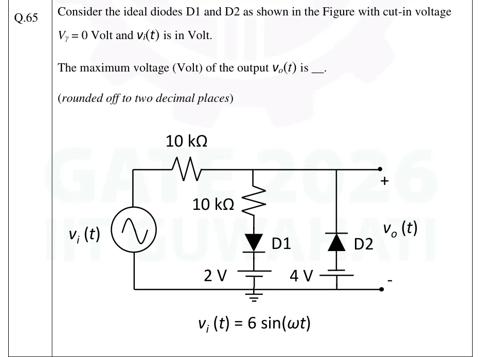
Consider the ideal diodes D1 and D2 as shown in the Figure with cut-in voltage Volt and is in Volt.

The maximum voltage (Volt) of the output is ____. (rounded off to two decimal places)
GATE 2026 EC question 65: A sinusoidal source v_i(t) = 6 sin (ω t) has its lower terminal on the bottom (ground) rail, which carries a ground symbol.Tap to open full size
Figure from the GATE 2026 EC paper. It is part of the question.
Figure description

A sinusoidal source v_i(t) = 6 sin (ω t) has its lower terminal on the bottom (ground) rail, which carries a ground symbol. Its upper terminal goes through a series 10 kΩ resistor to the top rail, and the top rail is the output node v_o(t) (+ at the top rail, − at the bottom rail). Two shunt branches run from the top rail down to the bottom rail. Branch 1: a 10 kΩ resistor, then diode D1 pointing downward (anode at the resistor, cathode below), then a 2 V battery with its long (+) plate on top, so D1's cathode sits at +2 V, and the battery's lower end on the ground rail. Branch 2, at the output: diode D2 pointing upward (cathode on the top rail, anode below), then a 4 V battery with its short (−) plate on top and its long (+) plate on the ground rail, so D2's anode sits at −4 V. Both diodes are ideal, with V_γ = 0.
Answer and solution
GATE 2026 EC Q.65: answer and solution

GATE 2026 EE Q.33

GATE 2026 · EEQ.33 · 1 mark · NAT

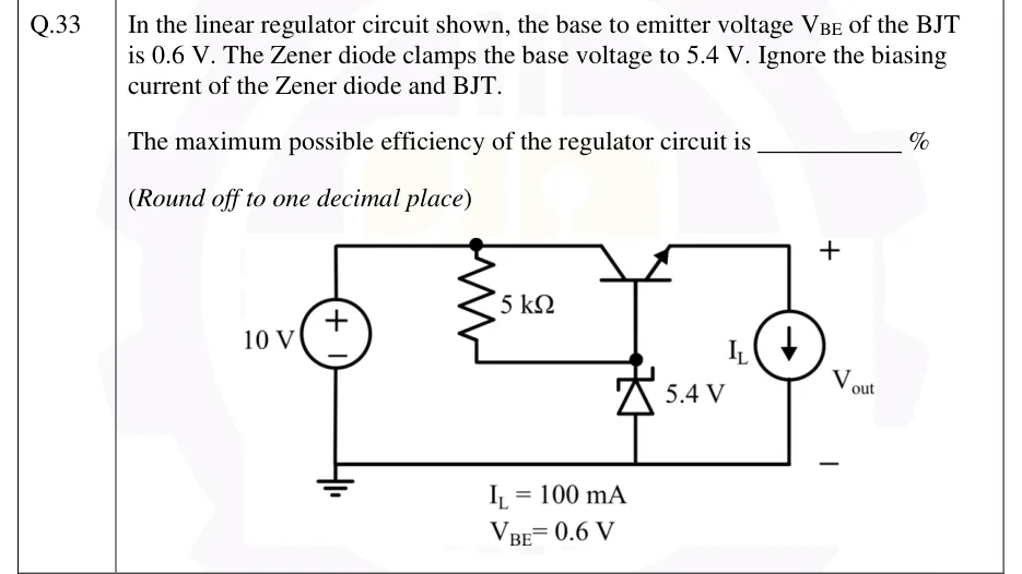
In the linear regulator circuit shown, the base to emitter voltage of the BJT is 0.6 V. The Zener diode clamps the base voltage to 5.4 V. Ignore the biasing current of the Zener diode and BJT.

The maximum possible efficiency of the regulator circuit is ________ %

(Round off to one decimal place)

(Figure data: , )

GATE 2026 EE question 33: Series-pass (emitter-follower) linear regulator.Tap to open full size
Figure from the GATE 2026 EE paper. It is part of the question.
Figure description

Series-pass (emitter-follower) linear regulator. A 10 V DC source (+ at top) has its negative terminal on the ground rail. The top rail from the source + goes to the collector of an NPN BJT (drawn horizontally: collector on the left, emitter on the right with the arrow pointing outward) and also to the top of a 5 kΩ resistor. The bottom of the 5 kΩ resistor connects to a node that goes up to the BJT base and down to the cathode of a Zener diode (anode to ground), labelled 5.4 V. The BJT emitter goes along the top right to an ideal DC current source I_L (arrow pointing down) whose lower terminal is on the ground rail; the output voltage V_out is taken across this current source, + at the top and − at the bottom. Labels under the circuit: I_L = 100 mA, V_BE = 0.6 V.

Answer and solution
GATE 2026 EE Q.33: answer and solution

GATE 2026 IN Q.34

GATE 2026 · INQ.34 · 1 mark · NAT

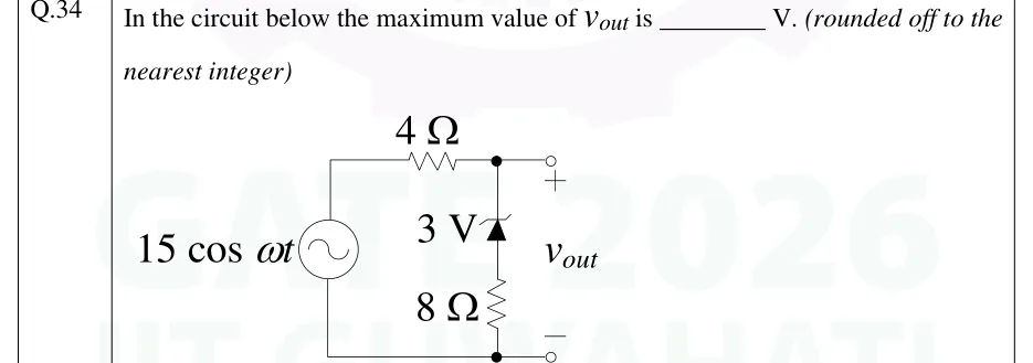
In the circuit below the maximum value of is ________ V. (rounded off to the nearest integer)

GATE 2026 IN question 34: An AC source 15 cos ω t (sinusoidal source symbol) on the left;Tap to open full size
Figure from the GATE 2026 IN paper. It is part of the question.
Figure description

An AC source 15 cos ω t (sinusoidal source symbol) on the left; its top terminal goes through a series 4 Ω resistor to the top output node (marked + of v_out). From the top output node to the bottom rail there is one branch: a 3 V Zener diode in series with an 8 Ω resistor. The Zener's cathode (bar with bent ends) is at the top, connected to the output node, and its triangle points upward, so the anode connects downward to the 8 Ω resistor, whose lower end goes to the bottom rail. The bottom rail returns to the source's lower terminal and is the - terminal of v_out. So v_out is measured across the Zener plus the 8 Ω resistor together. No load is connected at the output terminals.

Answer and solution
GATE 2026 IN Q.34: answer and solution

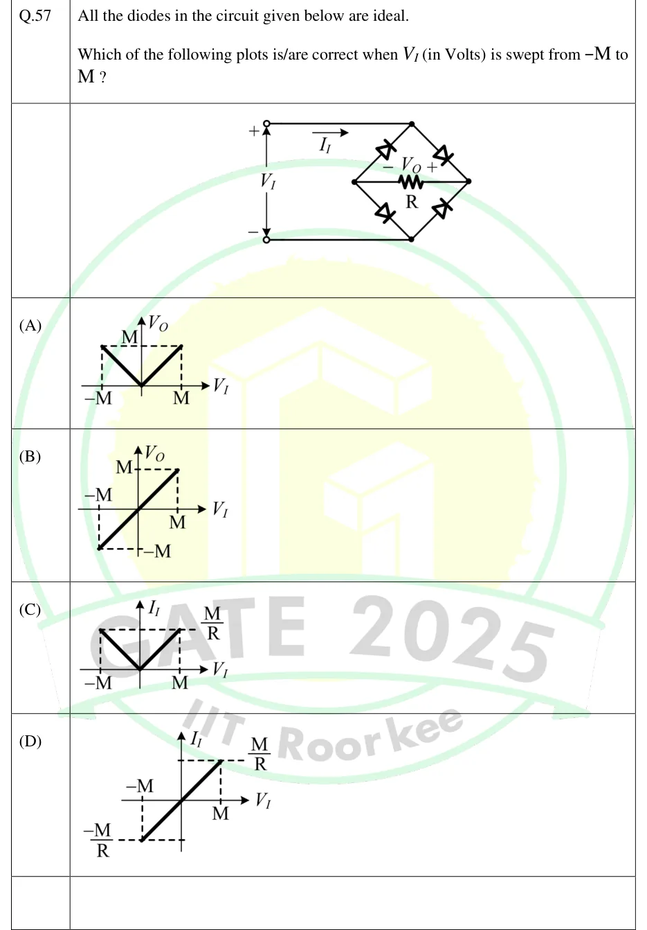
GATE 2025 EC Q.57

GATE 2025 · ECQ.57 · 2 marks · MSQ

All the diodes in the circuit given below are ideal.

Which of the following plots is/are correct when (in Volts) is swept from to ?

GATE 2025 EC question 57: A voltage source V_I with its + terminal at the top and its − terminal at the bottom.Tap to open full size
Figure from the GATE 2025 EC paper. It is part of the question.
Figure description

A voltage source V_I with its + terminal at the top and its − terminal at the bottom. The top wire goes from the + terminal to the top node T of a diamond-shaped bridge of four diodes. A current I_I is marked on this wire with its arrow pointing right, away from the source and into the bridge. The bottom wire goes from the − terminal to the bottom node B of the diamond. A resistor R is connected between the left node P and the right node Q of the diamond, and V_O is marked across it with − at P (left) and + at Q (right). The four ideal diodes are: upper-left, anode at P and cathode at T; upper-right, anode at T and cathode at Q; lower-left, anode at P and cathode at B; lower-right, anode at B and cathode at Q. So both diodes at Q have their cathodes there, and both diodes at P have their anodes there.

  1. (A)

    Figure — plot of (vertical axis) against (horizontal axis). It is V-shaped: at , it falls linearly to 0 at the origin, and it rises linearly back to at . Dashed lines mark the level M above .

  2. (B)

    Figure — plot of against . It is a straight line through the origin from to . Dashed lines mark at .

  3. (C)

    Figure — plot of against . It is V-shaped: at , it falls linearly to 0 at the origin, and it rises linearly back to at .

  4. (D)

    Figure — plot of against . It is a straight line through the origin from to . Dashed lines mark at .

Answer and solution
GATE 2025 EC Q.57: answer and solution

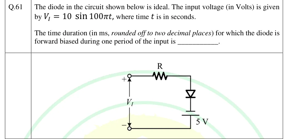
GATE 2025 EC Q.61

GATE 2025 · ECQ.61 · 2 marks · NAT

The diode in the circuit shown below is ideal. The input voltage (in Volts) is given by , where time is in seconds.

The time duration (in ms, rounded off to two decimal places) for which the diode is forward biased during one period of the input is ________.

GATE 2025 EC question 61: A single series loop.Tap to open full size
Figure from the GATE 2025 EC paper. It is part of the question.
Figure description

A single series loop. The input source V_I is shown between two open terminals on the left, with + at the top terminal and − at the bottom terminal. From the top (+) terminal a wire runs right through a resistor R to the top-right corner, then down into an ideal diode drawn vertically with its anode at the top (towards R) and its cathode at the bottom. Below the diode is a 5 V battery drawn vertically: its short plate (negative terminal) is at the top and connects to the diode cathode, and its long plate (positive terminal) is at the bottom and connects to the bottom wire. The bottom wire runs left back to the − terminal of V_I. So, taking the − terminal of V_I as reference, the diode cathode sits at -5 V.

Answer and solution
GATE 2025 EC Q.61: answer and solution

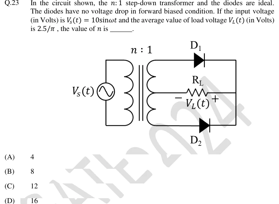
GATE 2024 EC Q.23

GATE 2024 · ECQ.23 · 1 mark · MCQ

In the circuit shown, the step-down transformer and the diodes are ideal. The diodes have no voltage drop in forward biased condition. If the input voltage (in Volts) is and the average value of load voltage (in Volts) is , the value of is ______.

GATE 2024 EC question 23: Center-tapped full-wave rectifier.Tap to open full size
Figure from the GATE 2024 EC paper. It is part of the question.
Figure description

Center-tapped full-wave rectifier. On the left an AC source V_s(t) is connected across the primary winding of an n:1 transformer (iron core, two parallel lines). The secondary winding has three terminals: top, a center tap and bottom. The top terminal goes to the anode of diode D_1. The bottom terminal goes to the anode of diode D_2. Both diodes point to the right, and their cathodes join a common vertical wire on the right. The center tap connects to the left end of load resistor R_L, and the right end of R_L connects to the common cathode wire. The load voltage V_L(t) is marked with - on the left (center-tap side) and + on the right (cathode side).

  1. (A)

    4

  2. (B)

    8

  3. (C)

    12

  4. (D)

    16

Answer and solution
GATE 2024 EC Q.23: answer and solution

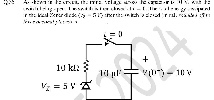
GATE 2024 EC Q.35

GATE 2024 · ECQ.35 · 1 mark · NAT

As shown in the circuit, the initial voltage across the capacitor is 10 V, with the switch being open. The switch is then closed at . The total energy dissipated in the ideal Zener diode () after the switch is closed (in mJ, rounded off to three decimal places) is ________.

GATE 2024 EC question 35: A single series loop.Tap to open full size
Figure from the GATE 2024 EC paper. It is part of the question.
Figure description

A single series loop. Right branch: a 10 µF capacitor, top plate marked +, bottom plate marked −, labelled V(0⁻) = 10 V. Top wire: a switch that closes at t = 0, joining the capacitor's top (+) terminal to the top of the left branch. Left branch, top to bottom: a 10 kΩ resistor, then a Zener diode labelled V_Z = 5 V. The Zener's triangle points upward with its bent (Zener) bar at the top, so the cathode connects to the resistor and the anode to the bottom wire. The bottom wire joins the Zener's anode to the capacitor's bottom (−) terminal.

Answer and solution
GATE 2024 EC Q.35: answer and solution

GATE 2024 EE Q.60

GATE 2024 · EEQ.60 · 2 marks · NAT

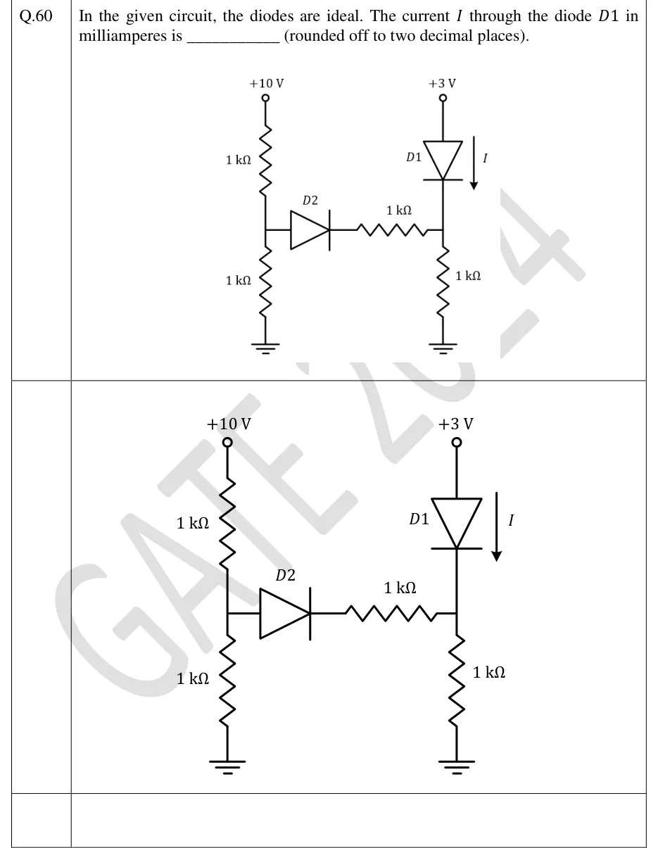
In the given circuit, the diodes are ideal. The current through the diode in milliamperes is ________ (rounded off to two decimal places).

GATE 2024 EE question 60: Left branch: a +10 V terminal feeds a 1 kΩ resistor down to node A, and a second 1 kΩ resistor runs from node A to ground.Tap to open full size
Figure from the GATE 2024 EE paper. It is part of the question.
Figure description

Left branch: a +10 V terminal feeds a 1 kΩ resistor down to node A, and a second 1 kΩ resistor runs from node A to ground. Diode D2 points to the right, with its anode at node A and its cathode going through a series 1 kΩ resistor to node B. Right branch: a +3 V terminal connects to the anode of diode D1, which points downward, so its cathode is at node B. The current I is marked by an arrow pointing downward through D1, from the +3 V terminal towards node B. Node B goes to ground through a 1 kΩ resistor.

Answer and solution
GATE 2024 EE Q.60: answer and solution

GATE 2024 IN Q.23

GATE 2024 · INQ.23 · 1 mark · NAT

Consider the circuit shown in the figure.

[Figure]

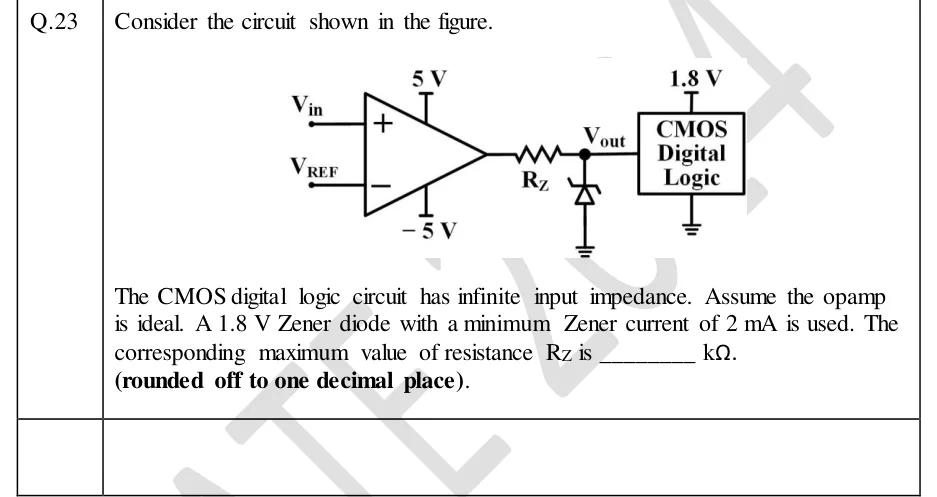
The CMOS digital logic circuit has infinite input impedance. Assume the opamp is ideal. A 1.8 V Zener diode with a minimum Zener current of 2 mA is used. The corresponding maximum value of resistance is ________ k. (rounded off to one decimal place).

GATE 2024 IN question 23: An op-amp used open-loop as a comparator.Tap to open full size
Figure from the GATE 2024 IN paper. It is part of the question.
Figure description

An op-amp used open-loop as a comparator. Input V_in goes to the non-inverting (+) input and V_REF to the inverting (−) input. The op-amp supply rails are +5 V (top) and −5 V (bottom). The op-amp output feeds one end of a series resistor R_Z. The other end of R_Z is the node labelled V_out. From V_out a Zener diode goes to ground, cathode at V_out and anode at ground, so it is reverse-biased when V_out is positive. V_out also drives the input of a block labelled 'CMOS Digital Logic', which is powered from 1.8 V at the top and grounded at the bottom.

Answer and solution
GATE 2024 IN Q.23: answer and solution

GATE 2024 IN Q.57

GATE 2024 · INQ.57 · 2 marks · NAT

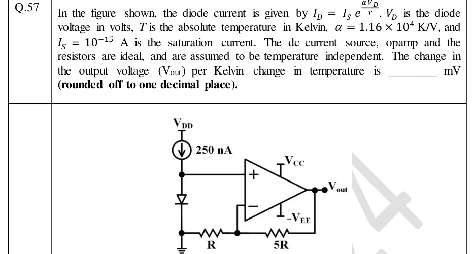
In the figure shown, the diode current is given by . is the diode voltage in volts, is the absolute temperature in Kelvin, , and is the saturation current. The dc current source, opamp and the resistors are ideal, and are assumed to be temperature independent. The change in the output voltage () per Kelvin change in temperature is ________ mV (rounded off to one decimal place).

GATE 2024 IN question 57: A 250 nA dc current source hangs from V_DD and drives its current downward into a node (call it A).Tap to open full size
Figure from the GATE 2024 IN paper. It is part of the question.
Figure description

A 250 nA dc current source hangs from V_DD and drives its current downward into a node (call it A). A diode runs from node A down to the bottom rail. The anode is at A and the cathode at the bottom rail, so the source current forward-biases it. The bottom rail is grounded. Node A also connects to the non-inverting (+) input of an op-amp powered from +V_CC and -V_EE. The op-amp output is V_out. A resistor 5R connects V_out to the inverting (-) input, and a resistor R connects the inverting (-) input to the grounded bottom rail (the diode's cathode). The circuit is a non-inverting amplifier that amplifies the diode voltage.

Answer and solution
GATE 2024 IN Q.57: answer and solution

GATE 2023 EC Q.40

GATE 2023 · ECQ.40 · 2 marks · MCQ

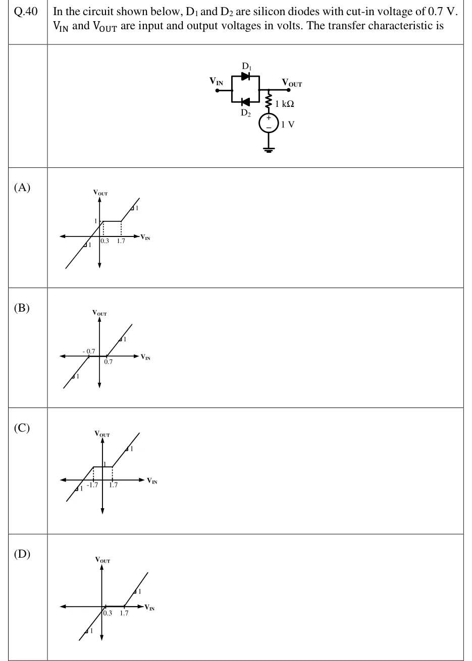
In the circuit shown below, and are silicon diodes with cut-in voltage of 0.7 V. and are input and output voltages in volts. The transfer characteristic is

GATE 2023 EC question 40: Input terminal V_IN on the left.Tap to open full size
Figure from the GATE 2023 EC paper. It is part of the question.
Figure description

Input terminal V_IN on the left. Between V_IN and the output node V_OUT are two diodes in antiparallel. D1 (top branch) has its anode at V_IN and its cathode at V_OUT, so it conducts from V_IN to V_OUT. D2 (bottom branch) has its anode at V_OUT and its cathode at V_IN, so it conducts from V_OUT to V_IN. From the V_OUT node, a 1 kΩ resistor goes down to the + terminal of a 1 V DC source. The source's − terminal goes to ground. Nothing else is connected to V_OUT, so the output is open-circuited.

  1. (A)

    Figure: V_OUT vs V_IN. V_OUT is flat at 1 for 0.3 ≤ V_IN ≤ 1.7 (dotted verticals drop from the flat section to V_IN = 0.3 and V_IN = 1.7). For V_IN > 1.7 it rises with slope 1. For V_IN < 0.3 it falls with slope 1 and crosses the V_IN axis at a negative V_IN.

  2. (B)

    Figure: V_OUT vs V_IN. V_OUT = 0 for −0.7 ≤ V_IN ≤ 0.7 (a dead zone on the V_IN axis). Outside that range it is a line of slope 1: rising for V_IN > 0.7 and falling below zero for V_IN < −0.7.

  3. (C)

    Figure: V_OUT vs V_IN. V_OUT is flat at 1 for −1.7 ≤ V_IN ≤ 1.7 (dotted verticals at −1.7 and 1.7). Outside that range it is a line of slope 1: rising for V_IN > 1.7 and falling for V_IN < −1.7.

  4. (D)

    Figure: V_OUT vs V_IN. V_OUT = 0 for 0.3 ≤ V_IN ≤ 1.7 (a flat segment on the V_IN axis). For V_IN > 1.7 it rises with slope 1. For V_IN < 0.3 it falls below zero with slope 1.

Answer and solution
GATE 2023 EC Q.40: answer and solution

GATE 2023 EE Q.44

GATE 2023 · EEQ.44 · 2 marks · MSQ

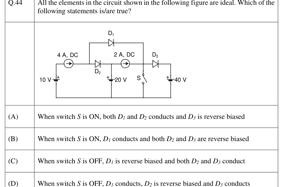
All the elements in the circuit shown in the following figure are ideal. Which of the following statements is/are true?

GATE 2023 EE question 44: A common bottom rail (ground) joins the negative terminals of three DC voltage sources and the lower contact of a switch.Tap to open full size
Figure from the GATE 2023 EE paper. It is part of the question.
Figure description

A common bottom rail (ground) joins the negative terminals of three DC voltage sources and the lower contact of a switch. Left branch: 10 V source, + at top; its top terminal feeds a 4 A DC current source whose arrow points right, into node P. From node P a wire rises to a top rail carrying diode D1 (anode on the left at P, cathode on the right), which comes back down at the right to node R. Also from node P, diode D2 (anode left at P, cathode right) goes along the middle rail to node Q. Node Q goes down to a 20 V source (+ at top, - to ground), and continues right through a 2 A DC current source (arrow pointing right, so current flows Q to R) to node R. At node R, the top rail from D1 comes down, switch S goes from R down to ground, and diode D3 (anode left at R, cathode right) goes right to the top of a 40 V source (+ at top, - to ground).

  1. (A)

    When switch S is ON, both D1 and D2 conducts and D3 is reverse biased

  2. (B)

    When switch S is ON, D1 conducts and both D2 and D3 are reverse biased

  3. (C)

    When switch S is OFF, D1 is reverse biased and both D2 and D3 conduct

  4. (D)

    When switch S is OFF, D1 conducts, D2 is reverse biased and D3 conducts

Answer and solution
GATE 2023 EE Q.44: answer and solution

GATE 2023 IN Q.33

GATE 2023 · INQ.33 · 1 mark · NAT

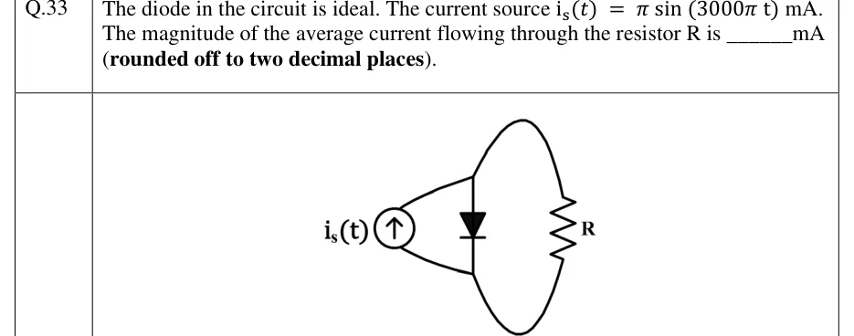
The diode in the circuit is ideal. The current source mA. The magnitude of the average current flowing through the resistor R is ______ mA (rounded off to two decimal places).

GATE 2023 IN question 33: Three elements connected in parallel between a top node and a bottom node: (1) on the left, an independent current source…Tap to open full size
Figure from the GATE 2023 IN paper. It is part of the question.
Figure description

Three elements connected in parallel between a top node and a bottom node: (1) on the left, an independent current source i_s(t) with its arrow pointing upward, so positive current is pushed into the top node; (2) in the middle, an ideal diode with its triangle pointing downward, meaning the anode is on the top node and the cathode is on the bottom node; (3) on the right, a resistor R. No other components are shown and R has no numerical value.

Answer and solution
GATE 2023 IN Q.33: answer and solution

GATE 2022 EC Q.57

GATE 2022 · ECQ.57 · 2 marks · NAT

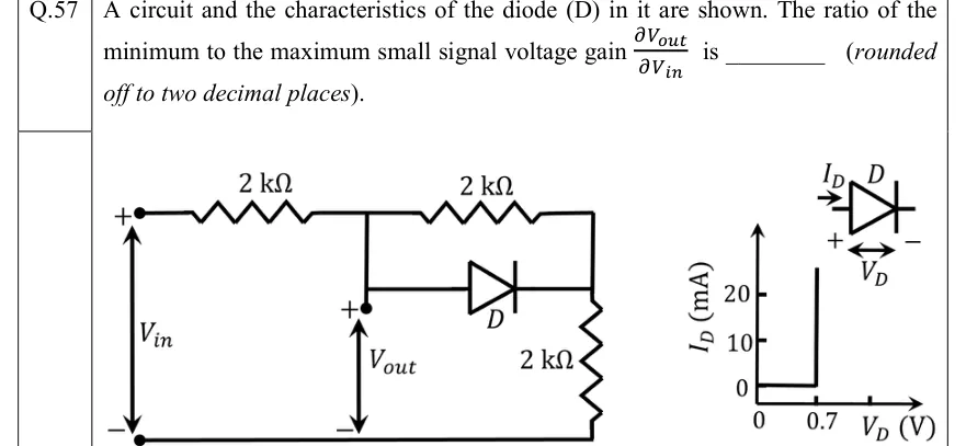
A circuit and the characteristics of the diode (D) in it are shown. The ratio of the minimum to the maximum small signal voltage gain is ________ (rounded off to two decimal places).

GATE 2022 EC question 57: Circuit: the input source V_in (+ on top, − at the bottom ground rail) feeds a series 2 k Ω resistor to node A.Tap to open full size
Figure from the GATE 2022 EC paper. It is part of the question.
Figure description

Circuit: the input source V_in (+ on top, − at the bottom ground rail) feeds a series 2 k Ω resistor to node A. V_out is taken at node A with respect to the bottom ground rail (+ at A). From node A two parallel branches go to node B: an upper 2 k Ω resistor, and below it diode D with its anode at A and its cathode at B (the triangle points from A toward B). From node B a 2 k Ω resistor goes down to the ground rail. Diode characteristic (right): I_D in mA on the vertical axis (ticks at 0, 10, 20), V_D in V on the horizontal axis (ticks at 0 and 0.7). I_D = 0 for V_D < 0.7 V, and at V_D = 0.7 V the curve rises vertically (any current at a fixed 0.7 V). The inset symbol defines I_D as the current entering the anode and V_D as the anode-to-cathode voltage (+ at the anode).

Answer and solution
GATE 2022 EC Q.57: answer and solution

GATE 2022 EE Q.25

GATE 2022 · EEQ.25 · 1 mark · MCQ

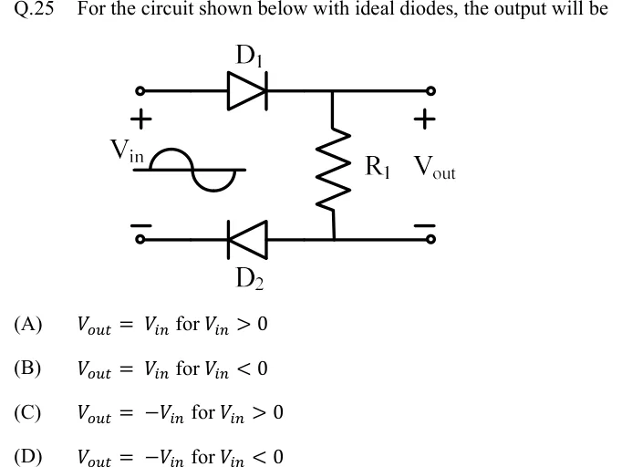
For the circuit shown below with ideal diodes, the output will be

GATE 2022 EE question 25: A sinusoidal source V_in (drawn as a sine-wave symbol) sits between two input terminals, with + marked on the upper…Tap to open full size
Figure from the GATE 2022 EE paper. It is part of the question.
Figure description

A sinusoidal source V_in (drawn as a sine-wave symbol) sits between two input terminals, with + marked on the upper terminal and - on the lower one. Upper wire: from the + input terminal to the anode of diode D_1. D_1 points right, so its cathode is on the right and connects to the top output node. Lower wire: from the - input terminal to the cathode of diode D_2. D_2 points left, so its anode is on the right and connects to the bottom output node. Resistor R_1 is connected vertically between the top output node and the bottom output node. V_out is taken across R_1, with + at the top output terminal and - at the bottom output terminal.

  1. (A)

    for

  2. (B)

    for

  3. (C)

    for

  4. (D)

    for

Answer and solution
GATE 2022 EE Q.25: answer and solution

GATE 2022 IN Q.31

GATE 2022 · INQ.31 · 1 mark · NAT

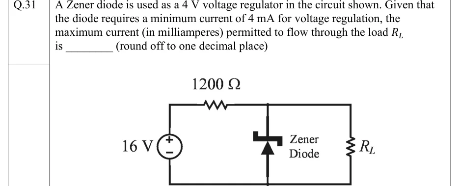
A Zener diode is used as a 4 V voltage regulator in the circuit shown. Given that the diode requires a minimum current of 4 mA for voltage regulation, the maximum current (in milliamperes) permitted to flow through the load is ________ (round off to one decimal place)

GATE 2022 IN question 31: A 16 V DC voltage source on the left, positive terminal at the top.Tap to open full size
Figure from the GATE 2022 IN paper. It is part of the question.
Figure description

A 16 V DC voltage source on the left, positive terminal at the top. From the top of the source, a series resistor of 1200 Ω runs along the top wire to a node. From that node two branches go down to the common bottom wire. The first is the Zener diode (labelled 'Zener Diode'), drawn with its cathode (bent bar) at the top node and its anode at the bottom wire, so the source reverse-biases it. The second is the load resistor R_L on the far right, in parallel with the Zener. The bottom wire returns to the negative terminal of the 16 V source.

Answer and solution
GATE 2022 IN Q.31: answer and solution

GATE 2022 IN Q.36

GATE 2022 · INQ.36 · 2 marks · MCQ

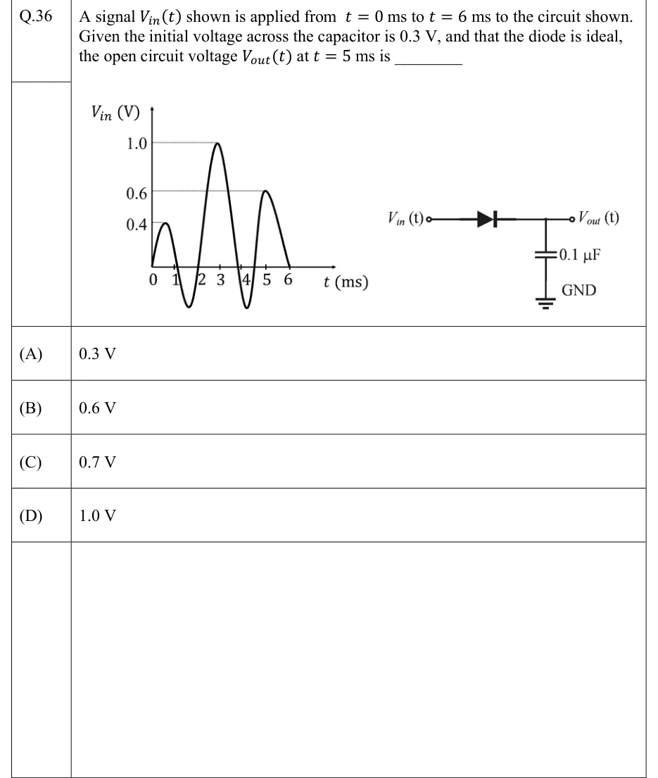
A signal shown is applied from ms to ms to the circuit shown. Given the initial voltage across the capacitor is 0.3 V, and that the diode is ideal, the open circuit voltage at ms is ________

GATE 2022 IN question 36: Left: plot of V_in (V) against t (ms).Tap to open full size
Figure from the GATE 2022 IN paper. It is part of the question.
Figure description

Left: plot of V_in (V) against t (ms). The time axis has ticks at t = 0, 1, 2, 3, 4, 5, 6 ms. Dotted horizontal reference lines run from the vertical axis at 0.4, 0.6 and 1.0 V, and each one ends at a peak of the waveform. The waveform starts at 0 V at t = 0 and rises to a positive peak of 0.4 V at about t = 0.5 ms. It crosses zero just after t = 1 ms and dips to an unlabelled negative minimum at about t = 1.5 ms. It crosses zero again just before t = 2 ms and rises to the largest peak, 1.0 V, just before t = 3 ms. It crosses zero at about t = 3.8 ms and dips to a second unlabelled negative minimum, drawn to the same depth as the first, at about t = 4.2 ms. It crosses zero at about t = 4.5 ms, reaches its last positive peak, 0.6 V, at t = 5 ms, and falls back to 0 V at t = 6 ms, where the curve ends. Right: circuit. The input terminal V_in(t) connects to the anode of a series diode pointing from input to output. The cathode connects to the output terminal V_out(t) and to one plate of a 0.1 µF capacitor. The capacitor's other plate goes to ground (GND). Nothing else is connected to the output (open circuit).

  1. (A)

    0.3 V

  2. (B)

    0.6 V

  3. (C)

    0.7 V

  4. (D)

    1.0 V

Answer and solution
GATE 2022 IN Q.36: answer and solution

GATE 2020 EC Q.17

GATE 2020 · ECQ.17 · 1 mark · NAT

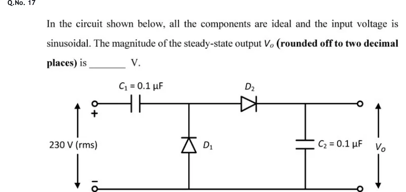
In the circuit shown below, all the components are ideal and the input voltage is sinusoidal. The magnitude of the steady-state output (rounded off to two decimal places) is ______ V.

GATE 2020 EC question 17: A two-stage diode-capacitor circuit (a half-wave voltage doubler).Tap to open full size
Figure from the GATE 2020 EC paper. It is part of the question.
Figure description

A two-stage diode-capacitor circuit (a half-wave voltage doubler). On the left are two open input terminals: the upper one is marked + and the lower one is marked -. A double-headed vertical arrow between them is labelled 230 V (rms). The lower input terminal feeds the common ground rail. The upper input terminal connects through series capacitor C1 = 0.1 uF to a middle node. Diode D1 is vertical between the ground rail and the middle node, with its anode at ground and its cathode (bar) at the middle node, so its triangle points up. Diode D2 runs from the middle node toward the output, with its anode at the middle node and its cathode toward the upper output terminal, so its triangle points right. Capacitor C2 = 0.1 uF connects the output node to the ground rail. The output V_o is taken across C2, between two open output terminals (upper and lower), and is marked with a double-headed vertical arrow.

Answer and solution
GATE 2020 EC Q.17: answer and solution

GATE 2020 EC Q.44

GATE 2020 · ECQ.44 · 2 marks · NAT

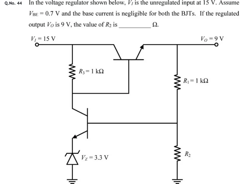
In the voltage regulator shown below, is the unregulated input at 15 V. Assume and the base current is negligible for both the BJTs. If the regulated output is 9 V, the value of is ________ .

GATE 2020 EC question 44: Series transistor voltage regulator.Tap to open full size
Figure from the GATE 2020 EC paper. It is part of the question.
Figure description

Series transistor voltage regulator. Input terminal V_I = 15 V at top left; output terminal V_O = 9 V at top right. Pass transistor Q1 (NPN) sits in the top line: collector connected to the V_I line, emitter (arrow pointing outward) connected to the V_O line, base pointing downward. From the V_I line, resistor R3 = 1 kΩ goes down to a node; that node connects to the base of Q1 and to the collector of a second NPN transistor Q2 (error amplifier). Q2 emitter (arrow outward) goes down to the cathode of a Zener diode V_Z = 3.3 V whose anode is grounded. On the output side, a voltage divider from V_O to ground: R1 = 1 kΩ on top, R2 at the bottom; the R1–R2 junction is connected by a horizontal wire to the base of Q2.

Answer and solution
GATE 2020 EC Q.44: answer and solution

GATE 2020 EE Q.31

GATE 2020 · EEQ.31 · 2 marks · MCQ

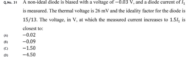
A non-ideal diode is biased with a voltage of , and a diode current of is measured. The thermal voltage is and the ideality factor for the diode is . The voltage, in V, at which the measured current increases to is closest to:

  1. (A)

  2. (B)

  3. (C)

  4. (D)

Answer and solution
See the question in the paper
GATE 2020 EE Q.31: answer and solution

GATE 2020 IN Q.7

GATE 2020 · INQ.7 · 1 mark · MCQ

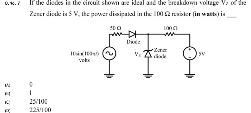
If the diodes in the circuit shown are ideal and the breakdown voltage of the Zener diode is 5 V, the power dissipated in the resistor (in watts) is ____

GATE 2020 IN question 7: An AC source 10 sin (100 π t) volts has its bottom terminal grounded.Tap to open full size
Figure from the GATE 2020 IN paper. It is part of the question.
Figure description

An AC source 10 sin (100 π t) volts has its bottom terminal grounded. From its top terminal a 50 Ω resistor runs to the right, then an ideal diode labelled "Diode" with its anode on the left (towards the resistor) and its cathode on the right, ending at a node. From this node a Zener diode labelled "Zener diode" (voltage marked V_Z) goes down to ground. The triangle points up and the bent bar is at the top, so the cathode is at the node and the anode is at ground. From the same node a 100 Ω resistor runs to the right to the + terminal of a 5 V DC source, whose - terminal is grounded.

  1. (A)

    0

  2. (B)

    1

  3. (C)

    25/100

  4. (D)

    225/100

Answer and solution
GATE 2020 IN Q.7: answer and solution

GATE 2020 IN Q.51

GATE 2020 · INQ.51 · 2 marks · NAT

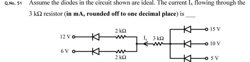
Assume the diodes in the circuit shown are ideal. The current flowing through the resistor (in mA, rounded off to one decimal place) is ____

GATE 2020 IN question 51: A central node X (left) and a node Y (right) are joined by a 3 kΩ resistor;Tap to open full size
Figure from the GATE 2020 IN paper. It is part of the question.
Figure description

A central node X (left) and a node Y (right) are joined by a 3 kΩ resistor; the current I_x is marked with an arrow pointing LEFT, i.e. from Y towards X, through the 3 kΩ resistor. Left side: two branches meet at node X. Upper branch: terminal '12 V' -> ideal diode -> 2 kΩ resistor -> node X, with the diode's cathode (bar) on the 12 V terminal side and its anode on the resistor side. Lower branch: terminal '6 V' -> ideal diode -> 2 kΩ resistor -> node X, again cathode towards the 6 V terminal and anode towards the resistor. Right side: node Y branches into three ideal diodes going to terminals '15 V' (top), '10 V' (middle) and '5 V' (bottom). Each of these diodes has its cathode (bar) on the node-Y side and its anode on the source-terminal side, so each can only pass current from its source into node Y. All terminal voltages are with respect to a common ground (not drawn).

Answer and solution
GATE 2020 IN Q.51: answer and solution

GATE 2018 EC Q.26

GATE 2018 · ECQ.26 · 2 marks · MCQ

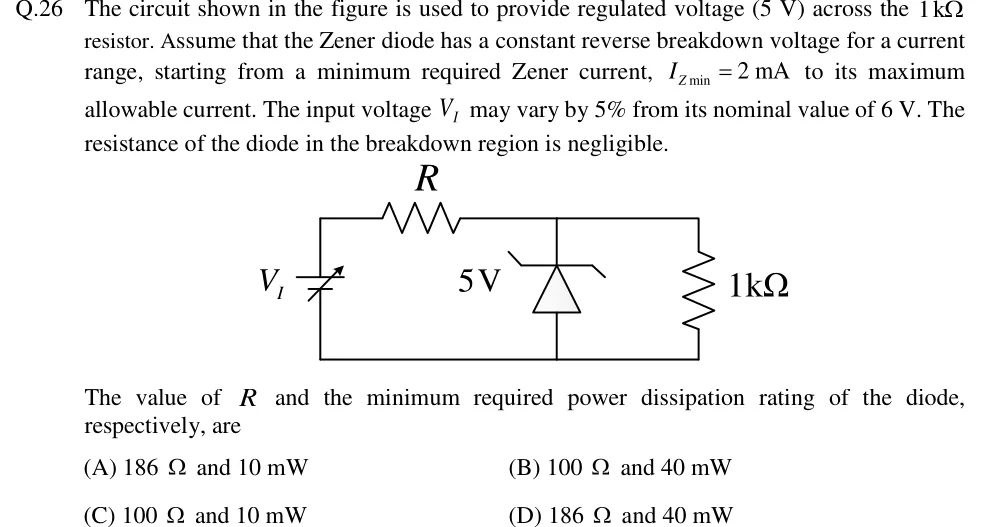
The circuit shown in the figure is used to provide regulated voltage (5 V) across the resistor. Assume that the Zener diode has a constant reverse breakdown voltage for a current range, starting from a minimum required Zener current, to its maximum allowable current. The input voltage may vary by 5% from its nominal value of 6 V. The resistance of the diode in the breakdown region is negligible.

The value of and the minimum required power dissipation rating of the diode, respectively, are

GATE 2018 EC question 26: Zener shunt regulator.Tap to open full size
Figure from the GATE 2018 EC paper. It is part of the question.
Figure description

Zener shunt regulator. A variable DC source V_I (battery symbol with a diagonal arrow, indicating it is variable) on the left, with its positive terminal at the top. From the top of the source, a series resistor R runs horizontally to the top node. Across the top node and the bottom (ground) rail are connected in parallel: a Zener diode labelled 5 V, drawn with its cathode (bar with bent ends) at the top node and anode at the bottom rail, so it is reverse-biased; and a 1 kΩ load resistor on the far right. The bottom rail connects the negative terminal of V_I, the Zener anode and the bottom of the 1 kΩ resistor.

  1. (A)

    186 Ω and 10 mW

  2. (B)

    100 Ω and 40 mW

  3. (C)

    100 Ω and 10 mW

  4. (D)

    186 Ω and 40 mW

Answer and solution
GATE 2018 EC Q.26: answer and solution

GATE 2018 EC Q.37

GATE 2018 · ECQ.37 · 2 marks · NAT

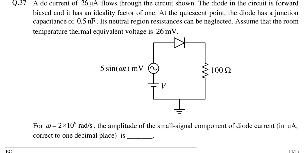
A dc current of flows through the circuit shown. The diode in the circuit is forward biased and it has an ideality factor of one. At the quiescent point, the diode has a junction capacitance of . Its neutral region resistances can be neglected. Assume that the room temperature thermal equivalent voltage is .

For , the amplitude of the small-signal component of diode current (in , correct to one decimal place) is ________.

GATE 2018 EC question 37: A single series loop.Tap to open full size
Figure from the GATE 2018 EC paper. It is part of the question.
Figure description

A single series loop. Left branch, from bottom to top: a dc battery labelled V (bottom plate connected to the bottom wire), and above it an ac sinusoidal source labelled 5 sin(ωt) mV. The top of the ac source connects by the top wire to the anode of a diode. The diode points to the right, so its anode is on the left and its cathode on the right. The cathode connects down the right branch through a 100 Ω resistor to the bottom wire. The bottom wire is connected to ground. The battery V is poled so that the diode is forward biased and carries the stated 26 µA dc current.

Answer and solution
GATE 2018 EC Q.37: answer and solution

GATE 2018 IN Q.16

GATE 2018 · INQ.16 · 1 mark · NAT

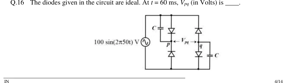
The diodes given in the circuit are ideal. At , (in Volts) is ____.

GATE 2018 IN question 16: A sinusoidal source 100 sin (2 π 50t) V on the left, connected between a top rail (call it A) and a bottom rail (call it B);Tap to open full size
Figure from the GATE 2018 IN paper. It is part of the question.
Figure description

A sinusoidal source 100 sin (2 π 50t) V on the left, connected between a top rail (call it A) and a bottom rail (call it B); no polarity marks are printed. Between the rails there are two vertical branches and two capacitors. Left branch: a diode from the top rail down to node p, triangle pointing down (anode on the top rail, cathode at p), and a diode from the bottom rail up to node p, triangle pointing up (anode on the bottom rail, cathode at p). A capacitor C runs from the top rail down to a wire that joins node p, so C sits between the top rail and p, directly across the upper diode. Right branch: a diode between node q and the top rail, triangle pointing up (anode at q, cathode on the top rail), and a diode from node q down to the bottom rail, triangle pointing down (anode at q, cathode on the bottom rail). A second capacitor C goes from node q (via a wire to the right) down to the bottom rail, so it sits directly across the lower right diode. An arrow labelled V_pq points between nodes p and q; nothing else is connected between p and q.

Answer and solution
GATE 2018 IN Q.16: answer and solution

PRACTICE

7 questions to test yourself

PRACTICE 11 mark · MCQ

A half-wave rectifier with an ideal diode is fed from V. A capacitor is connected directly across the load , with ms. In steady state, the peak inverse voltage across the diode is closest to

  1. (A)

    5 V

  2. (B)

    10 V

  3. (C)

    14.1 V

  4. (D)

    20 V

Answer and solution

Answer: (D)

  1. On the positive half-cycle the diode charges to the peak, V. Because ms, the capacitor stays at about 10 V.

  2. At the input's negative peak the anode is at V while the cathode is held at V.

  3. Reverse voltage V .

PRACTICE 22 marks · NAT

In a Zener shunt regulator, a 20 V dc source feeds a load through a series resistor, with a Zener diode connected across . In breakdown the Zener holds V (take ), and it regulates only while its current is at least 5 mA. The minimum value of (in ) for which the output stays regulated is ______ (round off to two decimal places).

Answer and solution

Answer: (accepted range )

  1. With the Zener in breakdown the output is 8 V, so mA whatever the load.

  2. The load may take at most mA.

  3. .

  4. Check: without the Zener, this load would sit at V V, so the Zener is indeed in breakdown.

PRACTICE 32 marks · MSQ

Consider full-wave centre-tapped and full-wave bridge rectifiers, both with ideal diodes and a resistive load, fed from a sinusoidal supply of frequency . Which of the following statements is/are correct?

  1. (A)

    For the same peak voltage across the load, the PIV rating per diode in the bridge is half that in the centre-tapped circuit.

  2. (B)

    The ripple factor of the bridge rectifier is about 0.48.

  3. (C)

    The transformer utilisation factor of the bridge rectifier is lower than that of the centre-tapped rectifier.

  4. (D)

    In both circuits, the fundamental frequency of the output ripple is .

Answer and solution

Answer: (A), (B), (D)

  1. (A) Bridge: each OFF diode sees . Centre-tapped: each half-secondary has peak , and the OFF diode sees the whole secondary, . True.

  2. (B) . True.

  3. (C) TUF is about 0.81 for the bridge and about 0.69 for the centre-tapped circuit (0.57 on the secondary alone), so the bridge's is higher. False.

  4. (D) Both conduct on every half-cycle, so the output repeats every and the ripple fundamental is . True.

PRACTICE 42 marks · MCQ

V is applied through a series capacitor to an output node. A shunt branch from the output node to ground contains a silicon diode in series with a 3 V battery: the diode's cathode is connected to the output node, its anode to the battery's negative terminal, and the battery's positive terminal is grounded. A resistor across the output satisfies . Using the constant-drop model with V, the steady-state output swings between

  1. (A)

    V and V

  2. (B)

    V and V

  3. (C)

    V and V

  4. (D)

    V and V

Answer and solution

Answer: (A)

  1. The anode sits at V. The diode is forward-biased when , i.e. V. So the output can never fall below V, and the bottom of the waveform is pinned there.

  2. In steady state the input's negative peak ( V) lands on V, so V.

  3. V, which swings from V to V. Check: the peak-to-peak is 10 V, equal to the input's.

  4. (B) is the ideal-diode answer; (D) adds the clamp magnitude of 3.7 V instead of the 1.3 V shift.

PRACTICE 52 marks · NAT

V drives a series resistor that feeds an output node. A load is connected from the output node to ground. In parallel with the load is a branch in which a diode has its anode at the output node and its cathode at the positive terminal of a 2 V battery whose negative terminal is grounded. Using the constant-drop model with V and no forward resistance, the peak current through the diode (in mA) is ______ (round off to one decimal place).

Answer and solution

Answer: (accepted range )

  1. The diode is ON when , i.e. V.

  2. With the diode OFF, the resistors form a divider: . So the diode starts to conduct at V, not at 2.7 V.

  3. While it is ON, V and , which is largest at V.

  4. At V: current in the series resistor mA, load current mA, so mA.

PRACTICE 61 mark · MCQ

Taking eV·µm, the longest wavelength of light that a silicon photodiode ( eV) can detect is closest to

  1. (A)

    0.65 µm

  2. (B)

    0.87 µm

  3. (C)

    1.11 µm

  4. (D)

    1.55 µm

Answer and solution

Answer: (C)

  1. A photon is absorbed across the gap only if its energy is at least , so the cut-off wavelength is .

  2. m m.

  3. Longer wavelengths, such as 1.55 µm, carry too little energy to be absorbed by silicon.

PRACTICE 71 mark · NAT

A full-wave rectifier with a capacitor-input filter runs from 50 Hz mains and supplies a load drawing an essentially constant 100 mA. Assume the capacitor discharges at this constant current for the whole interval between successive charging peaks, and neglect the conduction interval. For a peak-to-peak ripple of no more than 1 V, the minimum filter capacitance (in F) is ______.

Answer and solution

Answer: (accepted range )

  1. Full-wave: charging peaks occur every ms.

  2. Constant-current discharge: .

  3. F F.

OFFICIAL GATE 2027 SYLLABUS WORDING

Copied from the GATE 2027 syllabus; see all 2027 syllabi.

GATE EC

Diode Circuits: Clipping, clamping and rectifiers

GATE EE

Simple diode circuits: clipping, clamping, rectifiers

GATE IN

Types of diode and their applications

Preparing in Kolkata? IAE Academy's course for GATE ECE, GATE EE or GATE IN.