IAE Academy

GATE EC · EE · IN

Active filters and waveform circuits

Active filters, comparators, Schmitt triggers, timers, VCOs and PLLs

This topic covers the op-amp circuits that shape a signal's spectrum or turn it into switching and timing signals: first- and second-order active filters (Sallen-Key, Butterworth, band-pass, notch and all-pass), comparators and Schmitt triggers, op-amp and 555 multivibrators, square/triangle generators, VCOs and the phase-locked loop. Solving a question here comes down to reading the circuit correctly (which terminal gets the input and which gets the feedback), writing one node equation or threshold condition, and applying the matching standard result within its conditions.

13 previous-year questions · 12 solved · 5 practice questions

Conventions and first-order active filters

Conventions used throughout. Every op-amp is ideal unless a value is given: infinite open-loop gain, infinite input resistance (no current into either input), zero output resistance and unlimited bandwidth. In a filter the circuit has net negative feedback (a Sallen-Key filter also has a positive-feedback path through a capacitor, but it is stable for the gains given below), so the op-amp works in its linear region and (virtual short). In a comparator, Schmitt trigger or multivibrator it runs open loop or with positive feedback, so in general and the output sits at a rail: when and when . Saturation levels are symmetric, , unless stated. Diodes use the constant-drop model ( V when conducting) unless a diode is called ideal. is in rad/s and in Hz. A filter's cut-off frequency means the frequency at which its gain is 3 dB below the passband gain, unless stated.

Why active filters. A passive RC section is loaded by whatever follows it and cannot have gain. Building the RC network around an op-amp gives a passband gain set by resistors; the op-amp's input draws no current, so it does not load the RC network, and its near-zero output resistance means the next stage cannot load the filter. Sections can therefore be cascaded without interacting: the overall transfer function is simply the product of the stage transfer functions. (The source still sees the filter's own input impedance: for the non-inverting first-order low-pass below, that is .) No inductors are needed, even for second-order responses. The order of a filter is the degree of its denominator in ; a low-pass or high-pass of order n has an asymptotic roll-off of dB/decade (about dB/octave).

FIRST-ORDER LOW-PASS, NON-INVERTING

R in series from the input to the + terminal, C from the + terminal to ground; (− terminal to ground) and (output to − terminal) set the passband gain and do not affect . and . With (voltage follower), .

FIRST-ORDER HIGH-PASS, NON-INVERTING

R and C swap places: C in series to the + terminal, R from the + terminal to ground. , phase . A real op-amp's finite gain-bandwidth product eventually turns every active high-pass into a band-pass; the ideal model ignores this.

FIRST-ORDER LOW-PASS, INVERTING

from the input to the − terminal, in parallel with in the feedback path, + terminal grounded. Only the feedback pair sets . The passband phase is , so the total phase is .

FIRST-ORDER HIGH-PASS, INVERTING

and in series from the input to the − terminal, alone in the feedback path. Only the input pair sets ; the high-frequency gain is .

First-order low-pass response, relative to the passband gain

Gain relative to passband

Phase (non-inverting low-pass)

0.995

−0.04 dB

0.707

−3.01 dB

0.447

−6.99 dB

0.0995

−20.04 dB

EXAM TIP

In the inverting forms the cut-off comes from the RC pair that sits together: the feedback pair () for the low-pass, the input pair () for the high-pass. Using or is a common slip. In the non-inverting forms the gain resistors never affect .

Second-order filters: standard forms, Sallen-Key and Butterworth

Every standard second-order section has a denominator of the same form, ; only the numerator changes with the filter type. is the natural (pole) frequency and the quality factor; in control-systems language the damping ratio is . fixes the shape near : a low gives a gentle knee, a high a resonant peak. The poles are complex only for , and the low-pass magnitude peaks only for .

STANDARD SECOND-ORDER FORMS

K is the passband gain: at DC for the low-pass, at high frequency for the high-pass, at for the band-pass, and in both outer bands for the notch. . At : , and .

Type

Numerator

at

at

at

Low-pass

0

High-pass

0

Band-pass

0

0

Notch

0

PEAKING OF A SECOND-ORDER LOW-PASS

For the low-pass magnitude falls monotonically from K and has no peak. A high-pass with the same Q has the same peak value, at .

−3 DB FREQUENCY OF A SECOND-ORDER LOW-PASS

The frequency where , i.e. 3 dB below the DC gain K. It equals only when (Butterworth): (for example a unity-gain Sallen-Key with equal R and equal C) gives , and gives . For a high-pass with the same Q, . Do not take as the cut-off of a second-order filter unless its Q is .

Sallen-Key low-pass. Two resistors and run in series from the input to the + terminal. Capacitor goes from the junction of and to the op-amp output (the positive-feedback path) and goes from the + terminal to ground. The op-amp is a non-inverting amplifier of gain ( from the − terminal to ground, from the output to the − terminal); is a voltage follower. Nodal analysis at the junction and at the + terminal gives the result below.

SALLEN-KEY LOW-PASS (GENERAL)

is the capacitor to the output, the capacitor to ground; DC gain K. Dividing through by gives .

UNITY-GAIN SALLEN-KEY LOW-PASS (K = 1)

With equal resistors, Q is set by the capacitor ratio alone: Butterworth () needs , the feedback capacitor twice the grounded one. Equal R and equal C at unity gain give only .

EQUAL-COMPONENT SALLEN-KEY (LOW-PASS OR HIGH-PASS)

Holds for both the low-pass and the high-pass Sallen-Key; the gain alone sets Q. Stable only for : at the poles reach the axis and the circuit oscillates at , and for they are in the right half-plane. Butterworth: , i.e. . At the gain is .

Sallen-Key high-pass. Swap every resistor with a capacitor: and in series from the input to the + terminal, from their junction to the output, from the + terminal to ground. The amplifier is the same.

SALLEN-KEY HIGH-PASS (GENERAL)

is the resistor to the output, the resistor to ground, the input capacitor; high-frequency gain K. At unity gain with : , so Butterworth needs .

BUTTERWORTH MAGNITUDE RESPONSE

Low-pass of order n (for a high-pass, replace by ). Maximally flat at (the first derivatives of vanish there), no ripple, exactly −3 dB at for every n, asymptotic roll-off dB/decade, and phase at . The poles lie equally spaced on a circle of radius in the left half-plane. Other standard approximations make different trade-offs: Chebyshev accepts ripple in the passband for a sharper transition at the same order, and Bessel accepts a gentler transition for a nearly constant group delay; all three roll off at dB/decade asymptotically.

BUTTERWORTH ORDER REQUIRED

= the largest attenuation (dB) allowed at the passband edge ; = the least attenuation (dB) required at the stopband edge (low-pass: ; high-pass: use ). Round n UP to an integer. If is the −3 dB cut-off, . Example: at least 40 dB at needs , so .

BUTTERWORTH SECTION Q VALUES

Each complex-pole pair becomes one second-order section, all with . When n is odd, add one first-order section with its cut-off at .

Order n

Sections

Stage Q values

Equal-component Sallen-Key gains,

1

one first-order

—

—

2

one second-order

0.707

1.586

3

first-order + second-order

1.000

2.000

4

two second-order

0.541, 1.307

1.152, 2.235

5

first-order + two second-order

0.618, 1.618

1.382, 2.382

6

three second-order

0.518, 0.707, 1.932

1.068, 1.586, 2.482

Designing an equal-component Sallen-Key Butterworth stage

  1. Choose a convenient capacitor value C for both capacitors.

  2. Set both resistors to ; the same R serves a low-pass or a high-pass.

  3. Set from the table (1.586 for a single second-order Butterworth stage).

  4. Pick and set .

  5. The passband gain is then K, not 1. Because K fixes Q, it cannot be chosen freely; if another overall gain is needed, add an attenuator or a separate gain stage.

WORKED EXAMPLE · EXAMPLE 1: AN EQUAL-COMPONENT BUTTERWORTH LOW-PASS

Design a second-order Butterworth low-pass filter with a cut-off of 1 kHz using the equal-component Sallen-Key circuit with C = 10 nF and = 10 kΩ (ideal op-amp). Find R, , the passband gain in dB, the gain at 1 kHz, and the attenuation relative to the passband at 10 kHz.

Solution
  1. Equal components: , so kΩ (use 15.9 kΩ for both resistors).

  2. Butterworth needs , so and . Then kΩ.

  3. Passband (DC) gain , i.e. dB.

  4. At : , 3 dB below the passband, as every Butterworth response is at its cut-off.

  5. At 10 kHz: . Relative to the passband this is dB: 40 dB/decade for .

Answer: R = 15.9 kΩ (both), = 5.86 kΩ; passband gain 1.586 (4.0 dB); |H| = 1.12 at 1 kHz; 40 dB below the passband at 10 kHz.

EXAM TIP

In a Butterworth cascade the individual stages are not Butterworth: in a fourth-order design the stage peaks on its own, and only the product of the two stages is maximally flat. The overall passband gain is the product of the stage gains ( for the equal-component fourth-order design).

Band-pass, notch and all-pass filters

A band-pass filter passes the band between a lower cut-off and an upper cut-off . When the band is wide (), cascade a high-pass with cut-off and a low-pass with cut-off : the passband gain is then very nearly the product of the two stage gains, and each overall cut-off very nearly equals its own stage's cut-off. As the two cut-offs approach each other the stages interact. Two first-order stages with cut-offs make a second-order band-pass with centre , overall −3 dB bandwidth (not ), gain at equal to the product of the stage gains times , and , which can never exceed 1/2. For a narrow band (high Q), use a single second-order band-pass section such as the multiple-feedback (MFB) circuit below.

BAND-PASS RELATIONS

and are the −3 dB frequencies of the overall response. Exact for any second-order band-pass ( and ): the centre is the geometric, not the arithmetic, mean of the cut-offs. For a cascade of first-order stages, the stage cut-offs and are not the overall and unless (see above), although the gain always peaks at .

MULTIPLE-FEEDBACK BAND-PASS (EQUAL CAPACITORS)

Circuit: from the input to node A, from A to ground, one capacitor C from A to the − terminal and another C from A to the output, from the − terminal to the output, + terminal grounded. is the (inverting) gain at . BW and do not depend on , so tunes alone. A positive requires .

Notch (band-reject). A notch removes a narrow band around (for example 50 Hz mains hum) and passes everything else. Two common realisations: (i) a twin-T network (one T of two resistors R with a capacitor 2C to ground, in parallel with a T of two capacitors C with a resistor R/2 to ground), which gives a null at but on its own has only , so its grounded node is driven from a fraction of the buffered output to raise Q; (ii) subtracting a unity-centre-gain band-pass output from the input, which produces exactly the standard notch form. A wide-band reject filter is a low-pass (cut-off ) and a high-pass (cut-off ) in parallel, with their outputs summed.

NOTCH FROM A BAND-PASS

Zeros on the axis at give a true null (zero output) at ; the −3 dB rejection bandwidth is .

FIRST-ORDER ALL-PASS (PHASE SHIFTER)

The input drives both op-amp inputs: through to the − terminal (with from the output to the − terminal), and through R to the + terminal, with C from the + terminal to ground. Then and . The gain is 1 at every frequency; the phase goes from at DC through at towards . Swapping R and C gives , phase .

EXAM TIP

Do not take the centre frequency as the arithmetic mean. If the overall −3 dB frequencies of a second-order band-pass are kHz and kHz, kHz, not 5 kHz, and .

Comparators and Schmitt triggers

Comparator. An op-amp with no feedback compares with and swings to a rail. Apply the signal to one input and a reference to the other. With the signal on the + terminal (non-inverting comparator) the output is whenever ; with the signal on the − terminal (inverting comparator) the output is whenever . With the circuit is a zero-crossing detector: a sine input becomes a square wave of the same frequency with 50% duty cycle. A comparator with a non-zero reference is also called a level detector. Two comparators with references and their outputs combined form a window comparator, which indicates whether lies between and .

COMPARATOR (OPEN LOOP)

Ideal op-amp, no feedback: the virtual-short rule does NOT apply. If the output is limited by a series resistor followed by back-to-back Zener diodes from the limited output node to ground, the levels become (constant-drop diode model, V).

DUTY CYCLE OF A COMPARATOR DRIVEN BY A SINE WAVE

Non-inverting comparator, input , reference with ; D is the fraction of each period with the output at , and is in radians. For the inverting comparator the fraction is . gives exactly one half.

Practical limits. (1) With a finite open-loop gain , the input must differ from by at least to saturate the output (13 V / = 130 µV); this is the comparator's resolution. (2) The output cannot change faster than the slew rate SR, so a full swing takes about . (3) A slowly varying signal carrying noise crosses the reference several times near each crossing, so the output chatters. Positive feedback, the Schmitt trigger, cures (3) and also sharpens the transition.

Schmitt trigger (regenerative comparator). A fraction of the output is fed back to the + terminal. The feedback is positive, so the circuit has two stable states and the switching point depends on the present output: there is an upper threshold (crossed while the input rises) and a lower threshold (crossed while it falls). Their difference is the hysteresis width . Noise smaller than peak to peak cannot make the output chatter. In both circuits below, is the feedback resistor from the output to the + terminal.

INVERTING SCHMITT TRIGGER

Input to the − terminal; from the + terminal to the reference (ground if ), from the output to the + terminal. By superposition with . With : , , . The output goes LOW when rises above and HIGH when it falls below . The loop is centred at .

NON-INVERTING SCHMITT TRIGGER

Input through to the + terminal, from the output to the + terminal, reference on the − terminal (ground if ). Switching happens when reaches . With : and . The output goes HIGH when rises above and LOW when it falls below .

UNEQUAL SATURATION LEVELS

Inverting Schmitt trigger with and output levels and (the latter negative); the loop is then not centred on zero. For a Zener-limited output use the limited levels in place of the saturation levels.

Inverting Schmitt

Non-inverting Schmitt

Signal applied to

− terminal, directly

+ terminal, through

Thresholds with

Output for a large positive input

Rising input crossing sends the output

Low

High

Loop on the versus plot is traversed

Clockwise

Counter-clockwise

Current drawn from the signal source

None (ideal op-amp)

Flows through , so the source is loaded

Procedure for any positive-feedback switching circuit

  1. Check which terminal the feedback resistor returns to. The + terminal means positive feedback and a two-state circuit: do not use as a circuit law.

  2. Write (and ) by superposition in terms of , the input and any reference.

  3. The output switches at the instant ; solve that equation for the input voltage.

  4. Substitute for one threshold and for the other, then identify as the one crossed while the input rises.

  5. Trace the input waveform in time, switching the output only when the input crosses the threshold that belongs to the present output state.

WORKED EXAMPLE · EXAMPLE 2: A SCHMITT TRIGGER WITH A REFERENCE AND A SINE INPUT

An inverting Schmitt trigger uses = 10 kΩ from the + terminal to a reference V and = 20 kΩ from the output to the + terminal. The output saturates at ±12 V. The input is V. Find , , the hysteresis width, and the fraction of each period (in steady state) for which the output is at +12 V.

Solution
  1. Superposition at the + terminal: V.

  2. V gives V; V gives V. Hysteresis V, centred at 2 V.

  3. In steady state the input was last below −2 V (it reaches −10 V), so the output is at +12 V as the input rises. It goes low when rises through 6 V: .

  4. It returns high when the input falls through −2 V, on the falling part of the wave: .

  5. The output is low for of every and high for , a fraction .

Answer: = 6 V, = −2 V, = 8 V; the output is at +12 V for 57.0% of each period.

EXAM TIP

A resistor in series with the − terminal of an inverting Schmitt trigger carries no current and does not affect the thresholds; in the non-inverting circuit, is part of the divider and does. Use the saturation level actually given: if the question says the output saturates at ±13.5 V on ±15 V supplies, the thresholds use 13.5 V.

Op-amp multivibrators and square/triangle generators

A multivibrator is a two-state switching circuit. The bistable (two stable states) is the Schmitt trigger itself. The monostable has one stable state: a trigger flips it for a time set by an RC network, after which it returns. The astable has no stable state and oscillates freely, producing a square wave. All the timing in these circuits, and in the 555, comes from one fact: a capacitor charging through a resistor toward a target voltage.

RC TIMING (CHARGE OR DISCHARGE TOWARD A TARGET)

Time for a capacitor charging or discharging through R, from toward the asymptote , to reach (which must lie between the two). Every period and pulse-width formula in this section and the 555 section is this formula with specific values.

OP-AMP ASTABLE MULTIVIBRATOR

An inverting Schmitt trigger ( from the + terminal to ground, from the output to the + terminal) with R from the output to the − terminal and C from the − terminal to ground. With symmetric , each half-period the capacitor charges from toward until it reaches , so the output is a square wave with 50% duty cycle and T does not depend on . The capacitor voltage is a chain of exponential segments, not a true triangle. gives ; gives .

OP-AMP MONOSTABLE MULTIVIBRATOR

The astable above with a diode across C (anode at the − terminal) that clamps at (constant-drop model, V) while ; this stable state needs . A negative trigger pulse at the + terminal sends to ; C then charges from toward , and the circuit flips back when reaches . With and neglected, . After the pulse, C must recover to before the next trigger.

Square and triangle generator. A non-inverting Schmitt trigger drives an inverting integrator, and the integrator output is fed back as the Schmitt trigger's input. While the square wave is at the integrator output ramps down at the constant rate ; when it reaches the Schmitt trigger flips and the ramp reverses. The Schmitt trigger must be the non-inverting type because the integrator already inverts: each ramp must head toward the threshold that will flip it.

SQUARE/TRIANGLE GENERATOR

Schmitt trigger: from the triangle output to the + terminal, from the square output to the + terminal, − terminal grounded. Integrator: input resistor R, feedback capacitor C. The triangle swings between (peak-to-peak ; needs ) and the square between . From ; f is independent of because the ramp rate and the thresholds both scale with it.

Unequal ramp rates (for example two diode-steered integrator input resistors) give an asymmetric triangle and a square wave whose duty cycle is not 50%; making one slope much faster than the other gives a sawtooth. Making the ramp current proportional to an input voltage turns the circuit into a VCO (see the last section).

Type

Stable states

Trigger needed?

Output

Op-amp circuit

Bistable

2

Yes, to change state

A level that remembers the last threshold crossed

Schmitt trigger

Monostable (one-shot)

1

Yes

One pulse of fixed width T per trigger

Astable plus a clamp diode across C and a trigger input at the + terminal

Astable (free-running)

0

No

Continuous square wave

Schmitt trigger with RC feedback to the − terminal

The 555 timer

Inside the 555. Three equal internal resistors across set two references: for the threshold comparator (pin 6) and for the trigger comparator (pin 2). When the trigger pin falls below , the internal SR flip-flop is set: the output (pin 3) goes high and the discharge transistor (pin 7) turns off. When the threshold pin rises above , the flip-flop is reset: the output goes low and the discharge transistor turns on, pulling pin 7 to ground. Pin 5 (control voltage) sits at the upper reference, , and is normally bypassed to ground with a small capacitor; driving it to moves the references to and . Pin 4 (reset) is active-low and is tied to when unused.

555 MONOSTABLE PULSE WIDTH

R from to pins 6 and 7, C from there to ground, trigger on pin 2. In the stable state the output is low and C is held discharged. A trigger below sets the output high; C charges from 0 toward , and the pulse ends when . The trigger must return above before T ends (a narrow trigger pulse); in the basic circuit, further triggers during the pulse do not extend it. T does not depend on .

555 ASTABLE

from to pin 7, from pin 7 to pins 6 and 2, C from pins 6 and 2 to ground. C charges through and discharges through alone, between and (a ratio of 2 each way, hence ). With D defined as high time over period, D is always above one half and approaches it only when . must not be zero, or pin 7 shorts to ground when the discharge transistor turns on.

555 ASTABLE WITH A DIODE ACROSS R_B

A diode across (anode at pin 7) bypasses while C charges, so C charges through only and discharges through only. Ideal-diode result; with a real diode drop, comes out somewhat longer. gives a 50% duty cycle, and duty cycles below 50% become possible.

555 WITH THE CONTROL-VOLTAGE PIN DRIVEN

Pin 5 driven to moves the thresholds to and . is unaffected (the discharge still halves ), while raising lengthens and lowers f. This is how a 555 becomes a voltage-controlled oscillator and, in monostable mode, a pulse-width modulator. recovers the standard formulas.

EXAM TIP

Four 555 traps. (1) The first high time after power-up is longer, , because C starts from 0 instead of . (2) The basic astable cannot give a duty cycle of 50% or less (with D = high time/period); a question that needs one implies a diode, an inverter or a driven control pin. (3) Some questions define duty cycle as low time over period, so read the definition. (4) Changing alone does not change the timing, because the thresholds and the charging target scale together; changing does.

WORKED EXAMPLE · EXAMPLE 3: A 555 ASTABLE, THEN ITS CONTROL PIN DRIVEN

A 555 astable runs from V with = 4.7 kΩ, = 10 kΩ and C = 10 nF. (a) With pin 5 bypassed, find , , the frequency and the duty cycle (high time/period). (b) Pin 5 is now driven by a 6 V source. Find the new frequency and duty cycle.

Solution
  1. (a) µs and µs.

  2. µs, so kHz, and .

  3. (b) The thresholds become V and V. Charging from 3 V toward 12 V until 6 V: µs.

  4. Discharging from 6 V toward 0 until 3 V: µs, unchanged.

  5. µs, kHz and . Lowering below its normal V raised the frequency and here pushed the duty cycle below one half, which the resistor ratio alone never can.

Answer: (a) = 101.9 µs, = 69.3 µs, f = 5.84 kHz, D = 59.5%. (b) f = 7.76 kHz, D = 46.2%.

VCOs and the phase-locked loop

A voltage-controlled oscillator (VCO) produces a periodic output whose frequency is set by a control voltage . Over its useful range the characteristic is taken as linear about the free-running (centre) frequency . In a PLL, is the VCO frequency when the loop's control voltage is zero, i.e. at the VCO's bias point. Op-amp VCOs use the square/triangle generator with a ramp current proportional to ; a 555 becomes a VCO when its pin 5 is driven; LC oscillators are tuned by a varactor diode, whose capacitance falls as its reverse bias rises.

VCO CHARACTERISTIC

in Hz/V, in (rad/s)/V. Linear model. Check which unit a question uses before multiplying.

INTEGRATOR-SCHMITT VCO

An integrator (input resistor R, feedback capacitor C) whose input is switched between and by a Schmitt trigger of hysteresis width . Each half-period the ramp, of slope , crosses , so . The frequency is proportional to (), so this characteristic passes through the origin; used in a PLL, the VCO is biased so that zero loop control voltage gives .

Phase-locked loop. A PLL is a negative-feedback loop on phase, built from three blocks: a phase detector (PD), whose average output depends on the phase difference between the input and the VCO output; a loop filter (low-pass), which removes the PD's ripple at the sum frequency and sets the loop dynamics; and the VCO, driven by the filter output. When the loop is locked, the VCO frequency equals the input frequency exactly, because any remaining frequency difference would make the phase difference grow without limit. What remains is a constant phase error , just large enough to produce the control voltage that holds the VCO at the input frequency. is measured from the PD's zero-output point: for a multiplier with sine inputs and for an XOR detector, that point is a phase difference between the two inputs.

PHASE-DETECTOR CHARACTERISTICS

Multiplier of gain : inputs and average to , so V/rad ( for unit multiplier gain). XOR with logic levels 0 and : with 50% duty-cycle square waves a phase difference apart, the output is high for a fraction of the time, so V/rad; , measured from the midpoint output .

LOCKED LOOP: CONTROL VOLTAGE AND STATIC PHASE ERROR

Locked loop, linear PD model , loop-filter DC gain , so . (units 1/s) is the DC loop gain; the cancels if both the offset and the VCO gain are in Hz. A larger gives a smaller phase error for the same offset. With a sinusoidal PD, the second relation gives instead of .

LOCK (HOLD-IN) RANGE

is the largest PD output measured from its zero point: for the multiplier (at ), and for the XOR, whose characteristic is linear over . A loop that is already locked stays locked while the input moves up to this far from , i.e. as far as the largest available control voltage can pull the VCO (assuming the VCO itself can go that far). It depends on the filter's DC gain, not its bandwidth. Some questions quote the total width () instead of the one-sided value; read the wording.

CAPTURE (PULL-IN) RANGE, SINGLE-POLE RC LOOP FILTER

One-sided ranges; loop filter with ; an approximation valid when . Starting unlocked, the PD output is a beat at the difference frequency , which the filter attenuates by about ; the loop pulls in only if the attenuated beat still swings the VCO far enough, which gives . The capture range never exceeds the lock range. A narrower filter (larger ) narrows the capture range and leaves the lock range unchanged.

LINEARISED PLL PHASE MODEL

The VCO integrates frequency into phase, , so the open-loop gain always has a pole at the origin: a phase step leaves no steady-state error, while a frequency step leaves the constant static phase error above. With the loop is first-order with bandwidth rad/s; the single-pole filter makes it second-order, and a larger lowers both and .

Lock (hold-in, tracking) range

Capture (pull-in, acquisition) range

Starting condition

Loop already locked; the input drifts slowly

Loop unlocked when the input is applied

Set by

DC loop gain and the PD's output limit

DC loop gain and the loop filter's bandwidth

Effect of a narrower loop filter

None

Shrinks

Relation

The wider of the two

Never wider than the lock range

Applications. With a divide-by-N counter between the VCO and the PD, lock forces , so (frequency multiplication and synthesis; with a further divide-by-M on the reference input, ). With an FM input the VCO tracks the input frequency, so the control voltage is the demodulated message. Other uses include FSK demodulation, synchronous AM detection and clock recovery.

WORKED EXAMPLE · EXAMPLE 4: STATIC PHASE ERROR, LOCK RANGE AND CAPTURE RANGE

A PLL has a VCO with free-running frequency 500 kHz and gain = 50 kHz/V, a multiplier phase detector with V, and a single-pole RC loop filter with DC gain 1 and time constant = 1 ms. (a) The loop is locked to a 530 kHz input: find the control voltage and the static phase error. (b) Find the one-sided lock and capture ranges. (c) With the loop unlocked, a 520 kHz signal is applied. Does it lock?

Solution
  1. (a) Locked, so the VCO runs at 530 kHz and V.

  2. With : , so (0.848 rad). The small-angle model would give 0.75 rad, about 12% low.

  3. (b) The largest PD output is 0.8 V, so the VCO can be held within kHz of 500 kHz: lock range 460 kHz to 540 kHz.

  4. Capture: kHz, i.e. about 497.5 kHz to 502.5 kHz. Check: , so the approximation holds.

  5. (c) 520 kHz is inside the lock range but 20 kHz from the centre, far outside the ±2.52 kHz capture range, so the unlocked loop does not acquire it. Had the loop been locked at 500 kHz with the input then swept slowly up to 520 kHz, it would have stayed locked.

Answer: (a) = 0.6 V, = 48.6°. (b) Lock range ±40 kHz (460 kHz to 540 kHz); capture range about ±2.52 kHz. (c) No: 520 kHz is within the lock range but outside the capture range.

EXAM TIP

A locked PLL has zero frequency error, not zero phase error (with a simple RC filter or none). If a question asks for the VCO frequency in lock, it is the input frequency, times N if a divide-by-N sits in the feedback path; no calculation is needed. The control voltage and the phase error are where the numbers go.

PREVIOUS-YEAR QUESTIONS

13 questions from the EC and IN papers

Try each question first, then open the answer. One shows the official answer only. We placed each question under a topic ourselves; the exam paper does not label topics.

See these papers in full: GATE ECE 2025 · GATE ECE 2024 · GATE ECE 2022 · GATE ECE 2020 · GATE IN 2026 · GATE IN 2024 · GATE IN 2022 · GATE IN 2018

GATE 2026 IN Q.46

GATE 2026 · INQ.46 · 2 marks · MCQ

In the following active filter circuit with ideal op-amps, is , is , and has an amplitude of at .

The amplitude of is ________ V.
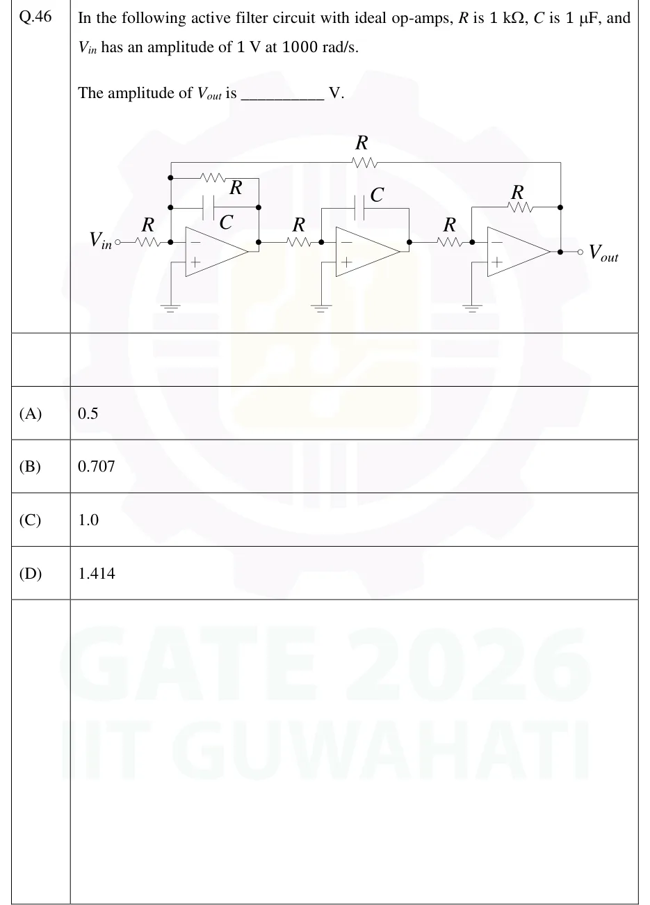
GATE 2026 IN question 46: Three ideal op-amps in cascade.Tap to open full size
Figure from the GATE 2026 IN paper. It is part of the question.
Figure description

Three ideal op-amps in cascade. Every non-inverting (+) input is grounded. Op-amp 1: V_in goes through a resistor R to the inverting (−) input. Between the inverting input and the output of op-amp 1 are a resistor R and a capacitor C in parallel. A further resistor R runs along the top of the circuit from the inverting input of op-amp 1 to the final output V_out, so it is a feedback path from the end of the chain. Op-amp 2: the output of op-amp 1 goes through R to the inverting input of op-amp 2. Capacitor C is the feedback element from the output of op-amp 2 to its inverting input, which makes an inverting integrator. Op-amp 3: the output of op-amp 2 goes through R to the inverting input of op-amp 3. Resistor R is the feedback element from the output to the inverting input, which makes a unity-gain inverter. The output of op-amp 3 is V_out.

  1. (A)

    0.5

  2. (B)

    0.707

  3. (C)

    1.0

  4. (D)

    1.414

Answer and solution
GATE 2026 IN Q.46: answer and solution

GATE 2026 IN Q.61

GATE 2026 · INQ.61 · 2 marks · NAT

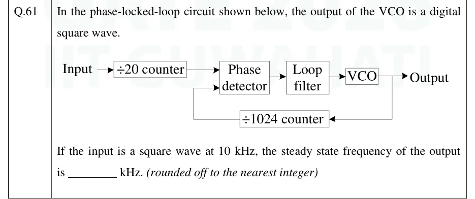
In the phase-locked-loop circuit shown below, the output of the VCO is a digital square wave.

If the input is a square wave at 10 kHz, the steady state frequency of the output is ________ kHz. (rounded off to the nearest integer)

GATE 2026 IN question 61: Block diagram of a PLL, left to right: 'Input' arrow into a '÷20 counter' block;Tap to open full size
Figure from the GATE 2026 IN paper. It is part of the question.
Figure description

Block diagram of a PLL, left to right: 'Input' arrow into a '÷20 counter' block; the counter output goes to one input of a 'Phase detector' block; the phase detector output goes to a 'Loop filter' block, then to a 'VCO' block; the VCO output is labelled 'Output'. Feedback path: the VCO output is tapped and fed back (right to left) through a '÷1024 counter' block, whose output goes to the second input of the phase detector.

Answer and solution
GATE 2026 IN Q.61: answer and solution

GATE 2025 EC Q.34

GATE 2025 · ECQ.34 · 1 mark · NAT

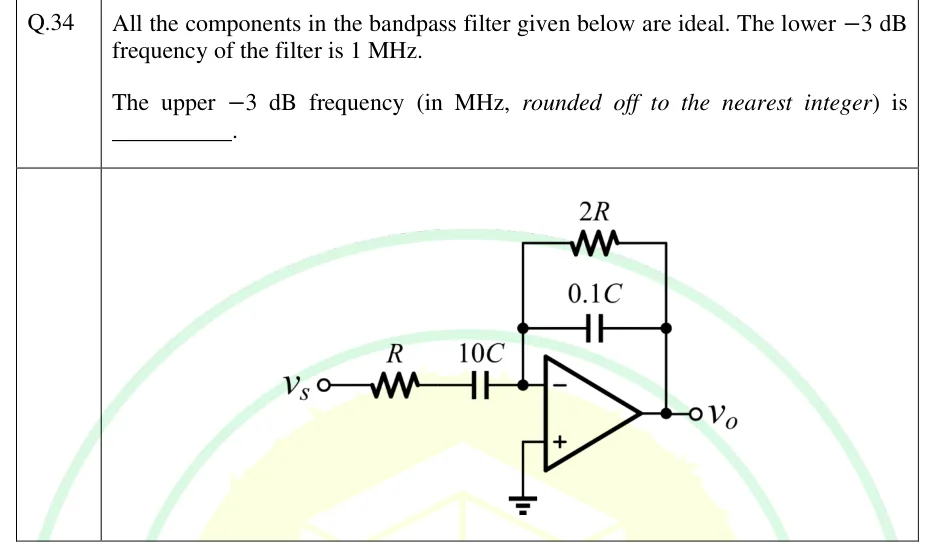
All the components in the bandpass filter given below are ideal. The lower dB frequency of the filter is 1 MHz.

The upper dB frequency (in MHz, rounded off to the nearest integer) is ________.

GATE 2025 EC question 34: Inverting op-amp bandpass filter.Tap to open full size
Figure from the GATE 2025 EC paper. It is part of the question.
Figure description

Inverting op-amp bandpass filter. The source v_s drives a series resistor R, which feeds a series capacitor 10C, and that capacitor connects to the op-amp's inverting (−) input. The non-inverting (+) input is grounded. The feedback network runs from the output v_o back to the inverting input and is a resistor 2R in parallel with a capacitor 0.1C. The output node is labelled v_o. No supply rails are drawn.

Answer and solution
GATE 2025 EC Q.34: answer and solution

GATE 2024 EC Q.49

GATE 2024 · ECQ.49 · 2 marks · MCQ

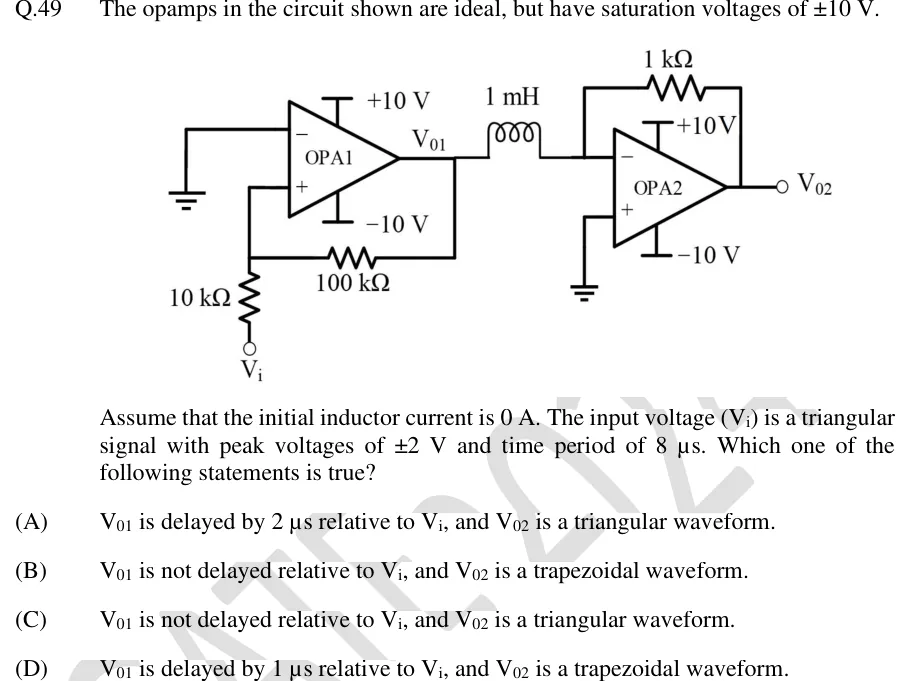
The opamps in the circuit shown are ideal, but have saturation voltages of .

[Figure]

Assume that the initial inductor current is . The input voltage () is a triangular signal with peak voltages of and time period of . Which one of the following statements is true?

GATE 2024 EC question 49: Two op-amp stages in cascade.Tap to open full size
Figure from the GATE 2024 EC paper. It is part of the question.
Figure description

Two op-amp stages in cascade. Stage 1 (OPA1), supplies +10 V and -10 V: its inverting (-) input is connected directly to ground. Its non-inverting (+) input is a node that connects (a) through a 10 kΩ resistor down to the input terminal V_i, and (b) through a 100 kΩ resistor to the OPA1 output, labelled V01 (positive feedback). Stage 2 (OPA2), supplies +10 V and -10 V: V01 drives a 1 mH inductor whose other end goes to the inverting (-) input of OPA2; the non-inverting (+) input of OPA2 is grounded; a 1 kΩ resistor connects the OPA2 output (terminal labelled V02) back to its inverting input.

  1. (A)

    is delayed by relative to , and is a triangular waveform.

  2. (B)

    is not delayed relative to , and is a trapezoidal waveform.

  3. (C)

    is not delayed relative to , and is a triangular waveform.

  4. (D)

    is delayed by relative to , and is a trapezoidal waveform.

Answer and solution
GATE 2024 EC Q.49: answer and solution

GATE 2024 IN Q.43

GATE 2024 · INQ.43 · 2 marks · MCQ

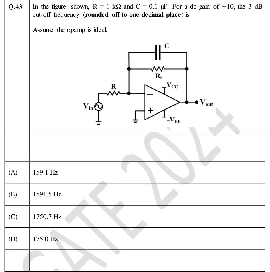
In the figure shown, and . For a dc gain of , the 3 dB cut-off frequency (rounded off to one decimal place) is

Assume the opamp is ideal.

GATE 2024 IN question 43: Inverting op-amp low-pass (integrator-type) filter.Tap to open full size
Figure from the GATE 2024 IN paper. It is part of the question.
Figure description

Inverting op-amp low-pass (integrator-type) filter. The source V_in (bottom terminal grounded) connects through resistor R to the inverting (−) input of the op-amp. The feedback network between the inverting input and the output node is a resistor R_f in parallel with a capacitor C (C drawn above R_f). The non-inverting (+) input is grounded. The op-amp is powered by V_CC (top) and -V_EE (bottom). The output node is labelled V_out.

  1. (A)

    159.1 Hz

  2. (B)

    1591.5 Hz

  3. (C)

    1750.7 Hz

  4. (D)

    175.0 Hz

Answer and solution
GATE 2024 IN Q.43: answer and solution

GATE 2024 IN Q.52

GATE 2024 · INQ.52 · 2 marks · NAT

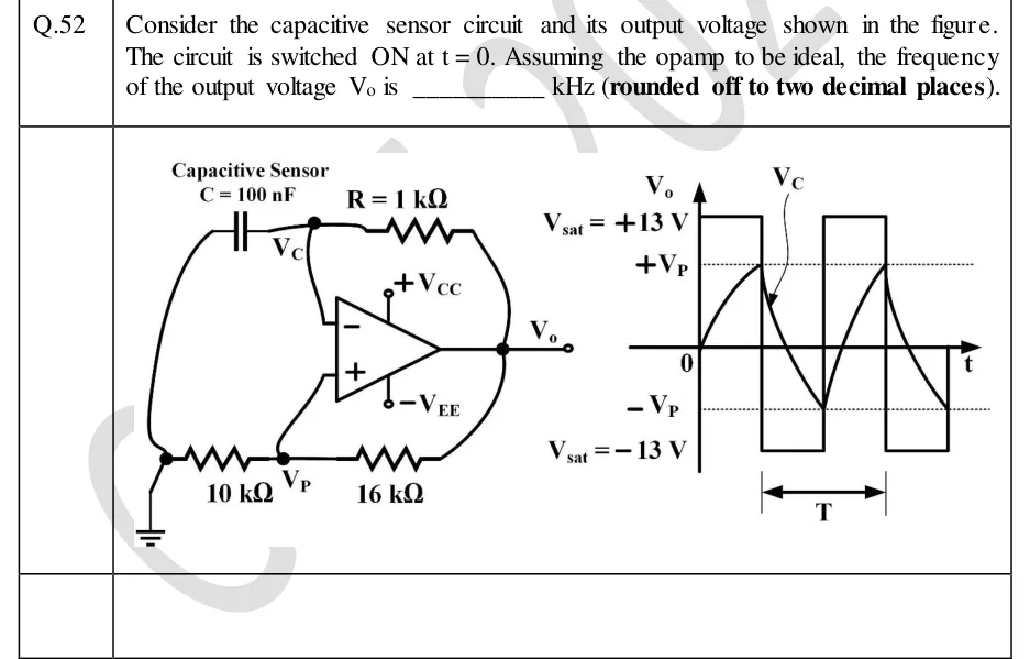
Consider the capacitive sensor circuit and its output voltage shown in the figure. The circuit is switched ON at . Assuming the opamp to be ideal, the frequency of the output voltage is ______ kHz (rounded off to two decimal places).

GATE 2024 IN question 52: Left: an op-amp astable (relaxation oscillator) with supplies +V_CC and -V_EE.Tap to open full size
Figure from the GATE 2024 IN paper. It is part of the question.
Figure description

Left: an op-amp astable (relaxation oscillator) with supplies +V_CC and -V_EE. A capacitive sensor C = 100 nF is connected between the inverting (−) input node, labelled V_C, and ground. A resistor R = 1 k Ω connects the V_C node to the output V_o (negative feedback path). The non-inverting (+) input node, labelled V_P, is connected to ground through a 10 k Ω resistor and to the output V_o through a 16 k Ω resistor (positive feedback). Right: waveform plot against t. V_o is a square wave switching between V_sat = +13 V and V_sat = -13 V. V_C starts at 0 at t = 0, rises exponentially to +V_P, then swings exponentially between +V_P and -V_P (dotted threshold lines), switching V_o each time it reaches a threshold. One period T is marked under the plot.

Answer and solution
GATE 2024 IN Q.52: answer and solution

GATE 2022 EC Q.26

GATE 2022 · ECQ.26 · 1 mark · MSQ

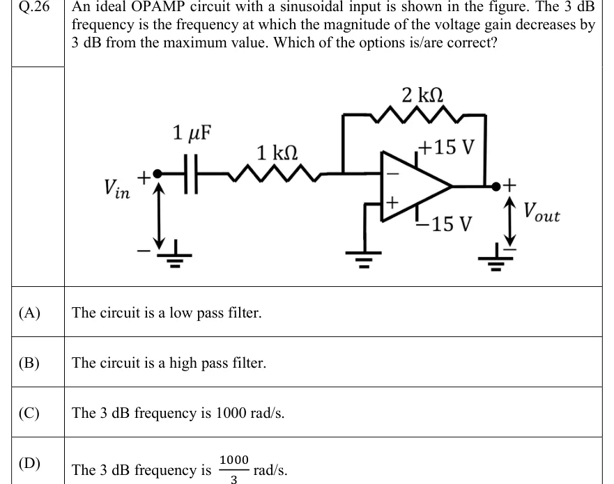
An ideal OPAMP circuit with a sinusoidal input is shown in the figure. The 3 dB frequency is the frequency at which the magnitude of the voltage gain decreases by 3 dB from the maximum value. Which of the options is/are correct?

GATE 2022 EC question 26: Inverting op-amp stage.Tap to open full size
Figure from the GATE 2022 EC paper. It is part of the question.
Figure description

Inverting op-amp stage. The source V_in (+ on top, - to ground) connects through a 1 capacitor and then a 1 k Ω resistor in series to the op-amp's inverting (-) input. A 2 k Ω feedback resistor goes from the op-amp output back to the inverting input. The non-inverting (+) input is grounded. The op-amp supplies are +15 V and -15 V. V_out is taken between the op-amp output (+) and ground (-).

  1. (A)

    The circuit is a low pass filter.

  2. (B)

    The circuit is a high pass filter.

  3. (C)

    The 3 dB frequency is 1000 rad/s.

  4. (D)

    The 3 dB frequency is rad/s.

Answer and solution
GATE 2022 EC Q.26: answer and solution

GATE 2022 EC Q.41

GATE 2022 · ECQ.41 · 2 marks · MCQ

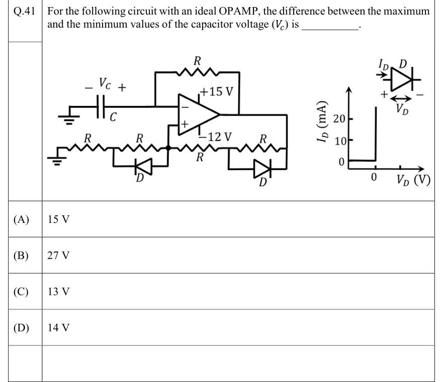
For the following circuit with an ideal OPAMP, the difference between the maximum and the minimum values of the capacitor voltage () is ________.

GATE 2022 EC question 41: An ideal op-amp with supply rails +15 V (top) and −12 V (bottom).Tap to open full size
Figure from the GATE 2022 EC paper. It is part of the question.
Figure description

An ideal op-amp with supply rails +15 V (top) and −12 V (bottom). Inverting (−) input: connected to one plate of capacitor C, whose other plate is grounded. The capacitor voltage is labelled V_C in the figure (V_c in the stem; the same quantity), with − on the ground side and + on the op-amp side, so V_C is the voltage at the inverting input. A resistor R runs from the op-amp output back to the inverting input, a negative-feedback path to the capacitor. Non-inverting (+) input: connected to node P (marked with a dot) on a horizontal resistor ladder between ground and the output. From left to right: ground, resistor R, node A, resistor R, node P, resistor R, node B, resistor R, then the op-amp output. A diode D sits across the A–P resistor with its anode at P and its cathode (bar) at A, so it conducts from P to A. A second diode D sits across the B–output resistor with its anode at B and its cathode (bar) at the output end, so it conducts from B to the output. A separate graph gives the diode characteristic, I_D (mA) against V_D (V), with an inset diode symbol: I_D enters the anode, and V_D is measured + at the anode to − at the cathode. The current is zero for V_D < 0 and rises vertically at V_D = 0. The I_D axis has ticks at 0, 10 and 20 mA; the V_D axis has a labelled tick at 0 and an unlabelled tick to its right. So the diode is ideal, with 0 V cut-in and zero on-resistance.

  1. (A)

    15 V

  2. (B)

    27 V

  3. (C)

    13 V

  4. (D)

    14 V

Answer and solution
GATE 2022 EC Q.41: answer and solution

GATE 2022 EC Q.42

GATE 2022 · ECQ.42 · 2 marks · MCQ

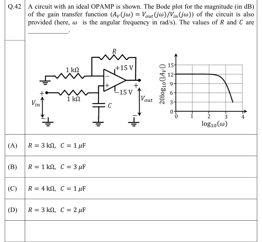
A circuit with an ideal OPAMP is shown. The Bode plot for the magnitude (in dB) of the gain transfer function of the circuit is also provided (here, is the angular frequency in rad/s). The values of and are ________.

GATE 2022 EC question 42: Left: the circuit.Tap to open full size
Figure from the GATE 2022 EC paper. It is part of the question.
Figure description

Left: the circuit. It uses an ideal op-amp with supply rails +15 V and −15 V. The inverting (−) input goes to ground through a 1 kΩ resistor, and a feedback resistor R connects the output to the inverting input. The non-inverting (+) input sits on a node that is fed from the source V_in (+ terminal) through a series 1 kΩ resistor. A capacitor C runs from that same node to ground. V_in is applied between the left end of the 1 kΩ series resistor (+) and ground (−). V_out is taken between the op-amp output (+) and ground (−). Right: the Bode magnitude plot. The vertical axis is 20log10(|A_V|) in dB, with dotted grid lines at 0, 3, 6, 9, 12 and 15. The horizontal axis is log10(ω), with grid lines at 0, 1, 2, 3 and 4. The curve is flat at 12 dB from log10(ω) = 0 to about 2. It then bends down gently, passes through the grid intersection at 9 dB and log10(ω) = 3, and keeps falling more steeply. The plotted curve ends at 3 dB near log10(ω) ≈ 3.4 to 3.5.

  1. (A)

  2. (B)

  3. (C)

  4. (D)

Answer and solution
GATE 2022 EC Q.42: answer and solution

GATE 2022 IN Q.56

GATE 2022 · INQ.56 · 2 marks · NAT

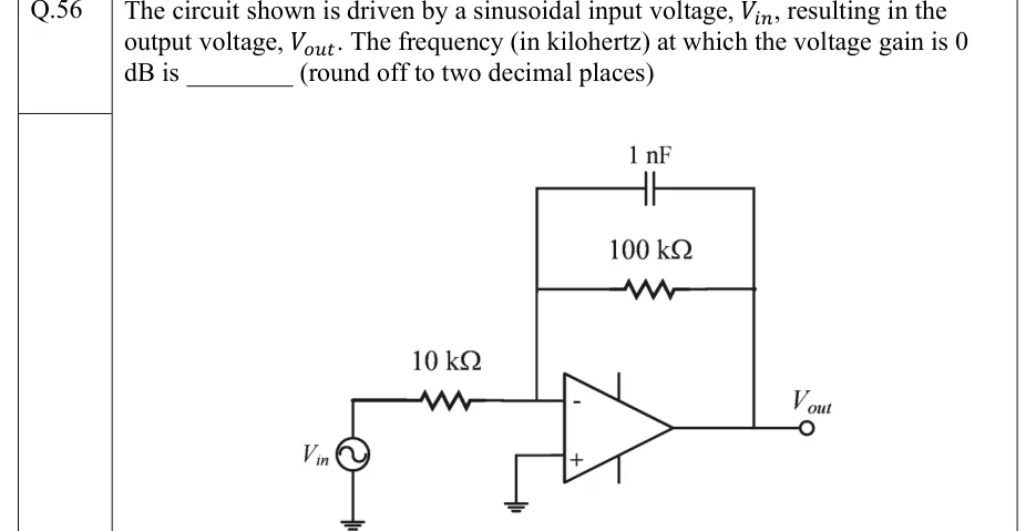
The circuit shown is driven by a sinusoidal input voltage, , resulting in the output voltage, . The frequency (in kilohertz) at which the voltage gain is 0 dB is ________ (round off to two decimal places)

GATE 2022 IN question 56: Inverting op-amp circuit.Tap to open full size
Figure from the GATE 2022 IN paper. It is part of the question.
Figure description

Inverting op-amp circuit. A sinusoidal source V_in has its lower terminal grounded and its upper terminal connected through a 10 kΩ resistor to the inverting (−) input of the op-amp. The non-inverting (+) input is grounded. The feedback network between the output and the inverting input is a 100 kΩ resistor in parallel with a 1 nF capacitor. The output node is labelled V_out. Supply rails are drawn as short stubs on the op-amp but have no values.

Answer and solution
GATE 2022 IN Q.56: answer and solution

GATE 2020 EC Q.8

GATE 2020 · ECQ.8 · 1 mark · MCQ

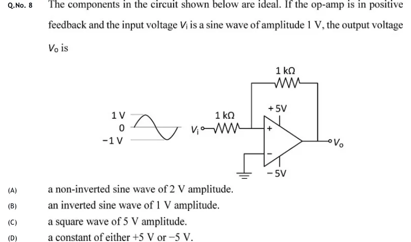
The components in the circuit shown below are ideal. If the op-amp is in positive feedback and the input voltage is a sine wave of amplitude 1 V, the output voltage is

GATE 2020 EC question 8: An op-amp with supply rails +5 V (top) and −5 V (bottom).Tap to open full size
Figure from the GATE 2020 EC paper. It is part of the question.
Figure description

An op-amp with supply rails +5 V (top) and −5 V (bottom). The input V_i is connected through a 1 kΩ resistor to the non-inverting (+) input, which is the upper input terminal. The inverting (−) input, the lower terminal, is connected to ground. A 1 kΩ feedback resistor runs from the output V_o back to the non-inverting (+) input node. To the left of V_i, a sketch shows the input waveform: a sine wave that swings between +1 V and −1 V about 0, with levels labelled 1 V, 0 and −1 V.

  1. (A)

    a non-inverted sine wave of 2 V amplitude.

  2. (B)

    an inverted sine wave of 1 V amplitude.

  3. (C)

    a square wave of 5 V amplitude.

  4. (D)

    a constant of either +5 V or −5 V.

Answer and solution
GATE 2020 EC Q.8: answer and solution

GATE 2020 EC Q.41

GATE 2020 · ECQ.41 · 2 marks · MCQ

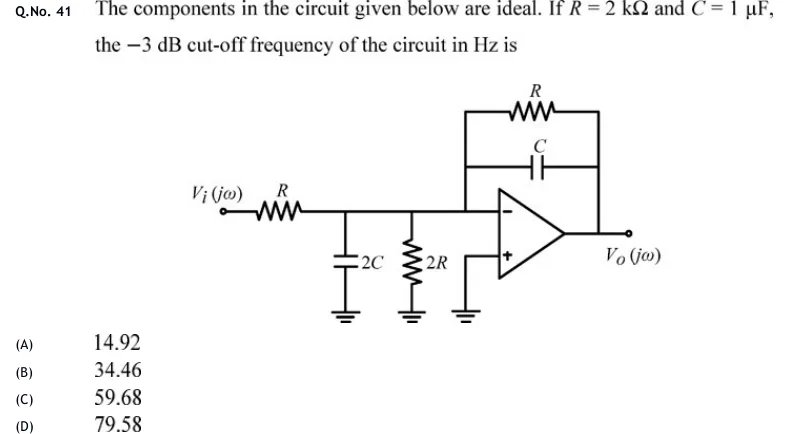
The components in the circuit given below are ideal. If and , the dB cut-off frequency of the circuit in Hz is

GATE 2020 EC question 41: Inverting op-amp circuit.Tap to open full size
Figure from the GATE 2020 EC paper. It is part of the question.
Figure description

Inverting op-amp circuit. Input source V_i(j ω) connects through a series resistor R to a node X. From node X to ground there are two shunt elements in parallel: a capacitor 2C and a resistor 2R. Node X connects directly to the inverting (−) input of an ideal op-amp. The non-inverting (+) input is connected to ground. The feedback network between the output and the inverting input (node X) is a resistor R in parallel with a capacitor C. The output is taken at the op-amp output terminal as V_o(j ω) with respect to ground.

Answer and solution
GATE 2020 EC Q.41: answer and solution

GATE 2018 IN Q.40

GATE 2018 · INQ.40 · 2 marks · NAT

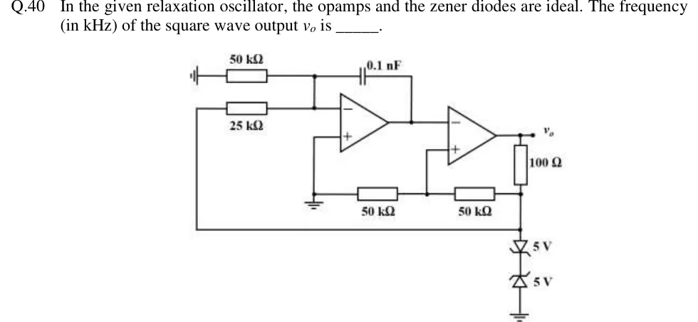
In the given relaxation oscillator, the opamps and the zener diodes are ideal. The frequency (in kHz) of the square wave output is ______.

GATE 2018 IN question 40: Two op-amps in cascade.Tap to open full size
Figure from the GATE 2018 IN paper. It is part of the question.
Figure description

Two op-amps in cascade. Op-amp 1 (integrator): its non-inverting (+) input goes straight to ground. Its inverting (−) input node connects to (i) a 50 kΩ resistor whose other end goes to a ground symbol drawn sideways at the far left, (ii) a 25 kΩ resistor whose other end is a wire that runs down the left side of the drawing and along the bottom to node A (described below), and (iii) a 0.1 nF capacitor running from the inverting input to the output of op-amp 1. Op-amp 2 (comparator): its inverting (−) input takes the output of op-amp 1. Its non-inverting (+) input goes to the junction of two 50 kΩ resistors in series along the bottom of the drawing. The left 50 kΩ goes to the ground line (the same line as op-amp 1's + input), and the right 50 kΩ goes to node A. The output of op-amp 2 is labelled v_o. From v_o, a 100 Ω resistor runs down to node A. From node A to ground there are two 5 V zener diodes back to back, joined cathode to cathode: the upper one has its anode at node A, the lower one has its anode at ground.

Official answer

Official answer: marks to all candidatesSource: Official answer key, GATE 2018 IN (IIT Guwahati)

GATE 2018 IN Q.40: official answer

PRACTICE

5 questions to test yourself

PRACTICE 11 mark · NAT

A 555 timer is wired as a monostable multivibrator with timing resistor R = 100 kΩ and timing capacitor C = 0.1 µF. The control-voltage pin is bypassed to ground through a capacitor and not otherwise driven, and the trigger pulse is much narrower than the output pulse. The width of the output pulse, in ms, is ______ (round off to two decimal places).

Answer and solution

Answer: (accepted range )

  1. With pin 5 not driven, the thresholds are (trigger) and (threshold).

  2. C charges from 0 toward and the pulse ends at : .

  3. ms (the rounded rule gives 11.0 ms).

PRACTICE 21 mark · MCQ

An inverting Schmitt trigger is built with an ideal op-amp whose output saturates at ±13 V. The input is applied to the inverting terminal; a 10 kΩ resistor connects the non-inverting terminal to ground, and a 90 kΩ resistor connects the output to the non-inverting terminal. The upper threshold , the lower threshold and the hysteresis width are

  1. (A)

    V, V, V

  2. (B)

    V, V, V

  3. (C)

    V, V, V

  4. (D)

    V, V, V

Answer and solution

Answer: (A)

  1. Feedback fraction , so .

  2. V gives V; V gives V.

  3. V. Option C uses the ratio 10/90 (the non-inverting Schmitt formula) and option D uses 90/100.

PRACTICE 32 marks · NAT

An equal-component Sallen-Key low-pass filter uses kΩ and nF. The ideal op-amp is connected as a non-inverting amplifier with = 10 kΩ from the inverting terminal to ground and = 12 kΩ from the output to the inverting terminal. The magnitude of the voltage gain at (about 1.59 kHz) is ______ (round off to two decimal places).

Answer and solution

Answer: (accepted range )

  1. Amplifier gain .

  2. Equal components: , so and .

  3. At the term cancels the constant: .

  4. The gain at exceeds the DC gain of 2.2 because , so the response peaks.

PRACTICE 42 marks · MSQ

A PLL has a VCO with free-running frequency 200 kHz and gain 25 kHz/V, with zero control voltage at the free-running frequency. Its phase detector gives an average output V ( in rad) for , and the loop loses lock if the required exceeds . The loop filter has a DC gain of 1. The loop is locked to a 210 kHz input. Which of the following statements is/are correct?

  1. (A)

    The VCO output frequency is 210 kHz.

  2. (B)

    The VCO control voltage is 0.4 V.

  3. (C)

    The static phase error is 0.2 rad.

  4. (D)

    Once locked, the loop can track the input, as the input frequency is varied slowly, over approximately 180.4 kHz to 219.6 kHz.

Answer and solution

Answer: (A), (B), (D)

  1. In lock the VCO frequency equals the input frequency, 210 kHz: A is correct.

  2. V: B is correct.

  3. rad, not 0.2 rad: C is wrong (0.2 comes from multiplying instead of dividing). Since , the loop does hold lock at 210 kHz.

  4. The largest control voltage is V, so the VCO can be held within kHz of 200 kHz, i.e. 180.4 kHz to 219.6 kHz: D is correct.

PRACTICE 52 marks · MCQ

A square/triangle generator uses a non-inverting Schmitt trigger followed by an inverting integrator, both built with ideal op-amps. In the Schmitt trigger, the integrator output is connected to the non-inverting terminal through = 10 kΩ, a resistor = 20 kΩ connects the Schmitt trigger's output to the same terminal, the inverting terminal is grounded, and the output saturates at ±12 V. The integrator is driven by the Schmitt trigger's output through an input resistor R = 10 kΩ and has a feedback capacitor C = 50 nF. The peak value of the triangular wave and the oscillation frequency are

  1. (A)

    6 V and 1 kHz

  2. (B)

    6 V and 2 kHz

  3. (C)

    24 V and 250 Hz

  4. (D)

    12 V and 1 kHz

Answer and solution

Answer: (A)

  1. The Schmitt trigger switches when , i.e. at V. The triangle swings between −6 V and +6 V: peak 6 V.

  2. The integrator ramps at V/s.

  3. Half-period ms, so ms and kHz. Check: Hz.

  4. Option C swaps and (and a 24 V peak is impossible with ±12 V rails).

OFFICIAL GATE 2027 SYLLABUS WORDING

Copied from the GATE 2027 syllabus; see all 2027 syllabi.

GATE EC

active filters, Schmitt trigger

GATE EE

single stage active filters, Active Filters: Sallen Key, Butterworth, VCOs and timers … Schmitt triggers

GATE IN

active filters, comparators, Schmitt trigger, multivibrators, oscillators, signal generators, voltage-controlled oscillators and phase-locked loop

Preparing in Kolkata? IAE Academy's course for GATE ECE, GATE EE or GATE IN.