IAE Academy

GATE EC · EE · IN

BJT and MOSFET biasing and DC analysis

Biasing sets a transistor's quiescent operating point (Q-point): the DC currents and voltages the signal swings about, and on which every small-signal parameter (, , ) depends. A GATE biasing question usually asks you to do three things. First, decide the region of operation by assuming one and checking it. Second, solve the bias loop, which is one linear equation for a BJT (constant-drop model) and a quadratic for a MOSFET (square law), where you must keep the root that leaves the device on. Third, judge how well the Q-point holds against changes in , , leakage and temperature, including the power the device dissipates.

13 previous-year questions · 13 solved · 6 practice questions

BJT regions, DC load line and Q-point

Conventions used in these notes. Transistors are npn unless stated. For a pnp, reverse every polarity and work with , and currents flowing out of the base and collector; all the npn equations then apply with positive numbers. The base-emitter junction uses the constant-drop model: V in the active region, and V with V in saturation. The Early effect is neglected (). Collector leakage (also written ) is neglected except when studying stability. Questions often give other values, such as 0.7 V for in every region, or V or 0.3 V. Always use the values the question gives.

A BJT has two junctions. Its region of operation depends on which of them is forward biased. DC analysis always follows the same pattern: assume a region, solve with that region's model, then check that the answer agrees with the assumption. Amplifiers are biased in the forward-active region. Switches use cut-off and saturation.

Region

B–E junction

B–C junction

Model used in DC analysis

Consistency check (npn)

Cut-off

Reverse (or below cut-in)

Reverse

The base loop cannot supply V (solving gives )

Forward active

Forward

Reverse

V,

and

Saturation

Forward

Forward

V, V

and , i.e.

Reverse active

Reverse

Forward

Collector and emitter swap roles; current gain

Not a bias condition used for amplifiers

TERMINAL CURRENTS IN THE ACTIVE REGION

Forward-active region only. With leakage included, . That is the form used to define the stability factor .

EXPONENTIAL MODEL OF THE ACTIVE REGION

Forward active with and the Early effect neglected. is the saturation current, proportional to the emitter area, and is the thermal voltage (25 mV or 26 mV at room temperature; use the question's value). The constant-drop model replaces this curve by a fixed . Each decade of collector current changes by : about 58 mV with mV, or 60 mV with mV. If an Early voltage is given, multiply by ; the output resistance is then .

Finding the region of a BJT (npn)

  1. Assume forward active. Put V and write KVL round the base loop to find (the master equation in the next section does this for every standard circuit).

  2. If this gives , the junction cannot turn on. The transistor is cut off: , and each node voltage follows from its resistors carrying zero current.

  3. Otherwise take and , and find from the collector loop.

  4. If , the assumption holds. The transistor is active and you have the Q-point.

  5. If , or comes out negative, the transistor is saturated. Put and , solve the base and collector loops (together if they share an emitter resistor), and confirm that and .

DC LOAD LINE

KVL round the collector loop, drawn on the – output characteristics, for circuits in which carries (in collector-feedback bias it carries ; see the next section). The intercepts are at (the cut-off end) and at . The approximate form takes (large ).

COLLECTOR CURRENT AT SATURATION

The largest collector current the external circuit allows, however hard the base is driven. With it is exact: . With present it assumes , which can be poor in saturation because the base current is no longer small compared with and also flows in ; for an exact answer solve the base and collector loops together.

The Q-point is where the load line crosses the output characteristic for the actual base current. The output can swing along the load line from up to . A Q-point close to saturation clips the half-cycle that drives down. A Q-point close to cut-off clips the half-cycle that drives towards zero. When the signal sees the same load as the DC circuit, the largest symmetrical swing comes from a Q-point at the middle of the load line, .

Q-POINT FOR MAXIMUM SYMMETRICAL SWING (AC LOAD LINE)

Use this when the signal-frequency load differs from the DC load. is the DC collector-loop resistance. is what the collector sees at signal frequencies, e.g. with bypassed. It places the Q-point at the middle of the AC load line, and neglects and leakage and takes . With it reduces to the midpoint, .

EXAM TIP

A computed that is positive but below (say 0.1 V) still means saturation. The test is , not . Once the check fails, drop : in saturation the collector current is set by the collector circuit alone.

BJT bias circuits

Every standard BJT bias circuit reduces (after a Thévenin step where needed) to one base loop: a source , a resistance in series with the base, the B–E drop, and a resistance that carries the emitter current . KVL round that loop gives one master equation. The circuits differ only in what , and are. A resistance carrying the emitter current appears in the base loop multiplied by . This 'reflection' is also why an emitter resistor stabilises the Q-point.

MASTER BASE-LOOP EQUATION (ACTIVE REGION)

npn, forward active, leakage neglected. Read , and for each circuit from the table below, then find from the collector loop and check that it exceeds .

Circuit

Fixed bias ( from to base, emitter grounded)

Emitter bias ( from , in emitter)

Collector-to-base (collector feedback), from collector to base

Voltage divider ( from to base, base to ground)

Two-supply emitter bias (base to ground via , to )

FIXED BIAS

is fixed by alone, so is directly proportional to . Changing the transistor, or its temperature, changes by the same fraction as changes.

COLLECTOR-TO-BASE (COLLECTOR-FEEDBACK) BIAS

runs from collector to base. carries , not . Put if there is no emitter resistor. If tries to rise, falls and so does : that is the negative feedback.

VOLTAGE-DIVIDER BIAS: EXACT (THÉVENIN) ANALYSIS

Exact within the constant-drop model. Use it whenever is given and the approximate condition below is not clearly met, or when the question asks how changes with .

VOLTAGE-DIVIDER BIAS: APPROXIMATE ANALYSIS

Ignores the base current's loading of the divider. Under the stated condition, , so is overestimated by less than 10% (and by a further factor ). The larger , the smaller the error. The result does not depend on , which is why this circuit gives a Q-point that is nearly independent of the transistor's .

TWO-SUPPLY EMITTER BIAS

Base returned to ground through , emitter to through . The approximation holds when . The emitter sits at , which is about when the drop is small (exactly with the base grounded directly).

WORKED EXAMPLE

An npn transistor with and V is biased from V by a divider: kΩ from to base and kΩ from base to ground. kΩ and kΩ. Find the Q-point exactly and compare it with the approximate method. Then find the stability factor and the power dissipated in the transistor.

Solution
  1. Thévenin equivalent of the divider: V and kΩ.

  2. Assume active: .

  3. mA and mA.

  4. V. This is above 0.2 V, so the transistor is active and the assumption holds.

  5. Approximate method: kΩ and kΩ, so the condition is only just met. mA and V. At the limit of the condition, the collector current comes out about 9% high.

  6. Stability: . Fixed bias with the same would give .

  7. Power: mW.

Answer: mA and V (the approximate method gives 1.7 mA and 3.5 V). and mW.

EXAM TIP

The approximate divider result does not contain . If a question asks how much changes when changes (say from 100 to 200), the approximate method would answer 'zero'. Use the exact Thévenin form instead.

EXAM TIP

A collector-to-base biased transistor (no other resistor at the base) cannot saturate while it conducts. With the base fed from the collector, , so the collector junction is never forward biased, and always exceeds . You can skip the saturation check for this circuit.

Stability factors S, S′ and S″

The collector current drifts with temperature through three parameters. The leakage roughly doubles for every 10 °C rise (a common rule of thumb). at constant current falls by roughly 2 to 2.5 mV/°C. rises with temperature and also varies widely between transistors of the same type. A stability factor is the sensitivity of to one of these parameters with the other two held constant. The smaller its magnitude, the more stable the Q-point. For , the ideal lower limit is 1.

DEFINITIONS OF THE STABILITY FACTORS

Each partial derivative holds the other two parameters constant. has no units, is in A/V and negative ( falls as rises), and is in A.

TOTAL DRIFT OF THE COLLECTOR CURRENT

First-order, for small changes. When temperature rises, and , so the term also increases . All three terms push the same way.

GENERAL EXPRESSION FOR S

Obtained by differentiating with respect to at constant . Get from the circuit's base-loop KVL. It is zero for fixed bias and negative whenever the circuit has feedback, which is what pulls below .

S FOR ANY CIRCUIT OF THE MASTER FORM

and come from the bias-circuit table. runs from for fixed bias () down to about when . A small ratio therefore means good stability.

S′ (SENSITIVITY TO V_BE)

Master form. Fixed bias: . Divider or emitter bias: when and .

S″ (SENSITIVITY TO Β), SMALL CHANGE

Master form, leakage neglected. For fixed bias (), , the largest possible for a given and .

S″ FOR A LARGE CHANGE OF Β

Exact within the master form (leakage neglected) when changes from to . is the collector current at , and is evaluated with . Then .

Circuit

Fixed bias

Emitter bias (, )

Collector-to-base ()

Voltage divider

, which is if

EXAM TIP

In collector-to-base bias (), plays the part of , but cannot be chosen freely. KVL gives , so once the Q-point is chosen that ratio, and with it , is fixed. For the ratio is 1, and , about half the fixed-bias value. In divider bias, can be made small without moving the Q-point (at the cost of more divider current), so can be brought much lower: 8.34 in the worked example above.

EXAM TIP

Compare stability factors of different circuits at the same . The negative feedback that lowers (an emitter resistor or collector feedback) also lowers the signal gain unless it is removed at signal frequencies, e.g. by bypassing with a capacitor. Bypassing does not change the DC stability.

BJT as a switch

As a switch, the transistor is driven between two states. OFF is cut-off: and . ON is saturation: and is set by the load. The active region is only passed through during switching. The design question is always the same: is the base drive large enough to guarantee saturation?

CONDITION FOR SATURATION

is the base current at the edge of saturation. Emitter grounded; with an emitter resistor, use and solve both loops together. To guarantee saturation for every device of a type, use .

FORCED BETA AND OVERDRIVE FACTOR

In saturation, the ratio is set by the external circuit, not by the transistor. The transistor is saturated when (ODF > 1). Designs deliberately keep well below for a margin.

MINIMUM INPUT VOLTAGE FOR SATURATION

Base driven from through , emitter grounded. At this input the transistor is at the edge of saturation. Some solutions use 0.7 V in place of ; follow the question.

EXAM TIP

Quick test for fixed bias with returned to the same : the transistor saturates when . That is, when , roughly when exceeds . A larger , a larger or a smaller all push the transistor towards saturation.

EXAM TIP

With the emitter grounded, the base and collector loops of a saturated transistor are independent. Find from the base loop with , and from the collector loop with . The static dissipation is small in either state: about zero when OFF, and when ON. The dissipation during the transitions is not included in these figures.

MOSFET regions of operation

Conventions. Enhancement NMOS unless stated, with the long-channel square law and in A/V². The threshold voltage is written to keep free for the thermal voltage. Overdrive is . Channel-length modulation is neglected () unless a value is given. The source is tied to the body (no body effect) unless stated. The gate draws no DC current (), so a gate bias network is never loaded by the transistor. Cut-off: for there is no channel and (subthreshold current neglected).

TRIODE (LINEAR, OHMIC) REGION

The channel exists all the way from source to drain. The current depends on both and .

SATURATION REGION

The channel is pinched off at the drain end. With , does not depend on , and the triode and saturation equations agree at the boundary , where . When is given, the small-signal output resistance is .

SATURATION TEST FROM TERMINAL VOLTAGES

Equivalent to (NMOS, device on). Handy when node voltages are known: the drain may sit at most below the gate. If , a channel exists at the drain end as well and the device is in triode.

DEEP-TRIODE ON RESISTANCE

The term is negligible here, so the MOSFET behaves as a resistor controlled by . This is the ON resistance of a MOSFET switch.

DEPLETION NMOS

For a depletion NMOS, (often written ). A channel already exists at , and is the saturation current there. The same triode and saturation equations and tests apply. may be negative (depletion mode) or positive (enhancement mode).

ENHANCEMENT PMOS

Here and . Current flows from source to drain. In triode (), . Working with , and keeps every quantity positive, and the NMOS rules carry over unchanged.

BODY EFFECT

NMOS whose source is above its body (). is the threshold at , is the body-effect coefficient (in V) and is the substrate's Fermi potential; use the symbols the question gives. The threshold rises as rises, which lowers at a given .

Device

Threshold

Conducts when

Saturated when

Enhancement NMOS

Depletion NMOS

(on at )

Enhancement PMOS

Depletion PMOS

(on at )

EXAM TIP

Check how the question defines its parameter. is the process parameter and the device parameter. Some write with . Putting in where is meant, or the reverse, gives a factor-of-2 error in .

EXAM TIP

The region test uses only voltages. and scale the current but never decide the region by themselves when and are known. In the symmetric device the square law describes, source and drain are interchangeable: in an NMOS the drain is whichever of the two terminals is at the higher potential, so relabel if the circuit puts the labelled 'drain' lower.

MOSFET biasing and diode-connected transistors

Because , the gate voltage comes straight from the gate network. A divider gives exactly, with no loading correction. Every standard arrangement then gives one bias line, , and combining it with the saturation equation gives a quadratic. A source resistor stabilises the Q-point. If tries to rise (a lower or a higher ), rises, falls and the rise is opposed. Fixed bias has no such feedback. There follows every spread in and directly.

Circuit

Remarks

Fixed bias (gate divider, source grounded)

; no feedback

Voltage divider with source resistor

The standard stable bias

Self bias (gate to ground through )

Works only for depletion devices; an enhancement NMOS stays off

Drain feedback ( from drain to gate, source grounded)

, so always saturated when on

Two supplies (gate grounded, to )

BIAS LINE AND THE ROOT THAT KEEPS THE DEVICE ON

This is the positive root of , assuming saturation, and . It needs ; otherwise the device is off. Afterwards, check . With , simply .

DC analysis of a MOSFET bias circuit

  1. Find from the gate network, using .

  2. Assume saturation and write .

  3. Solve the quadratic and keep the root with (). It is always the smaller . The larger root gives , which describes a device that would be off, where the square law does not apply.

  4. Find and , then check (equivalently ).

  5. If the check fails, the device is in triode. Redo step 2 with the triode equation on the same bias line, and keep the root with and .

WORKED EXAMPLE

An enhancement NMOS has V, mA/V² and . It is biased from V by a gate divider MΩ, with kΩ and kΩ. Find , , the region, and the power dissipated in the transistor.

Solution
  1. V. There is no gate current, so the divider is unloaded.

  2. Assume saturation. With in mA and kΩ, and .

  3. , so and mA or 9 mA.

  4. mA gives V, which is below , so the device would be off. Reject it. mA gives V and V. As a cross-check, the closed form with V gives V.

  5. V and V, so V. This is at least V, so saturation is confirmed.

  6. mW.

Answer: mA, V, saturation, mW.

Diode-connected transistors. Tying the gate of a MOSFET to its drain, or the base of a BJT to its collector, turns the device into a two-terminal element. It carries whatever current is forced through it and develops the matching or . Such devices are used as bias references (the input side of a current mirror), level shifters and active loads.

DIODE-CONNECTED MOSFET

Gate tied to drain (enhancement device, ). Since , it can never enter triode. Its small-signal resistance is (in parallel with if one is given; body effect neglected), where .

DIODE-CONNECTED BJT

Base tied to collector. The collector junction has zero bias, so it is not forward biased and still holds. The small-signal resistance is (hybrid- model with and ), with thermal voltage mV at room temperature (use 26 mV if the question does).

CURRENT MIRROR BUILT ON A DIODE-CONNECTED DEVICE

The diode-connected device sets (or ) for a second device. The MOSFETs share and and differ only in ; the BJTs are identical (same and ), so . Valid while the output device stays saturated (MOSFET) or active (BJT), with and the Early effect neglected.

EXAM TIP

Drain-feedback bias behaves like a diode connection at DC. With there is no drop across , so , and an enhancement NMOS in this circuit is saturated whenever it conducts. No region check is needed.

EXAM TIP

Self bias (, resistor in the source) cannot turn on an enhancement NMOS, because . If a question shows this circuit with an enhancement device, the device is off and . For a depletion device the same bias line gives a valid Q-point: keep the root with , i.e. .

Power dissipation, junction temperature and thermal runaway

DC POWER DISSIPATED IN THE DEVICE

Quiescent power turned into heat in the transistor. The base term is usually negligible. A MOSFET has no gate term because .

POWER DRAWN FROM THE SUPPLY

This includes the bias-divider current as well as the collector (drain) current. The supply power equals the power in all the resistors plus the power in the transistor.

MAXIMUM DEVICE DISSIPATION ON A RESISTIVE LOAD LINE

for a BJT (DC load line, ). For a MOSFET, replace by , by and by , with . is a parabola in that peaks at the midpoint of the load line.

JUNCTION TEMPERATURE

is the thermal resistance from junction to ambient, in °C/W. With a heat sink, (junction to case, case to sink, sink to ambient).

Thermal runaway. In a BJT, a rise in junction temperature raises and and lowers , and all three raise . If the higher increases the dissipation, the junction heats further. The loop runs away, and can destroy the device, unless the heat path removes the extra heat faster than it is produced. A MOSFET biased well above threshold is far less prone to this: carrier mobility falls with temperature, so drops as the device heats. Near threshold, the falling can dominate instead, so this protection is not guaranteed there.

CONDITION FOR THERMAL STABILITY

Dissipation must grow with junction temperature more slowly than the heat path can carry the extra heat away. Low stability factors keep small.

SELF-STABILISING Q-POINT

Here with and . With a Q-point below the midpoint of the load line, a rise in lowers , so runaway cannot start whatever the value of .

EXAM TIP

The midpoint is both where a symmetric-swing design puts the Q-point and where device dissipation peaks at . If the Q-point can drift along the load line, rate the transistor against , not against the Q-point power alone.

PREVIOUS-YEAR QUESTIONS

13 questions from the EC, EE and IN papers

Try each question first, then open the answer. We placed each question under a topic ourselves; the exam paper does not label topics.

See these papers in full: GATE ECE 2026 · GATE ECE 2025 · GATE ECE 2018 · GATE EE 2024 · GATE EE 2023 · GATE EE 2018 · GATE IN 2026 · GATE IN 2025 · GATE IN 2024 · GATE IN 2022 · GATE IN 2018

GATE 2026 EC Q.18

GATE 2026 · ECQ.18 · 1 mark · MCQ

Consider the circuit shown in the Figure with and .

Assume and for the BJT.

Which of the following options is the correct value of the current ?
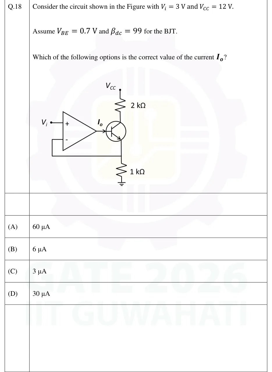
GATE 2026 EC question 18: An op-amp whose non-inverting (+) input is driven by the input voltage V_i and whose inverting (−) input is tied by a wire…Tap to open full size
Figure from the GATE 2026 EC paper. It is part of the question.
Figure description

An op-amp whose non-inverting (+) input is driven by the input voltage V_i and whose inverting (−) input is tied by a wire to the emitter of an NPN BJT. The op-amp output drives the BJT base directly; the current flowing out of the op-amp output into the base is labelled I_o (arrow pointing into the base). The BJT collector connects through a 2 k Ω resistor to the supply V_CC. The BJT emitter connects through a 1 k Ω resistor to ground, and the same emitter node is fed back to the op-amp's inverting input.

  1. (A)

  2. (B)

  3. (C)

  4. (D)

Answer and solution
GATE 2026 EC Q.18: answer and solution

GATE 2026 EC Q.60

GATE 2026 · ECQ.60 · 2 marks · NAT

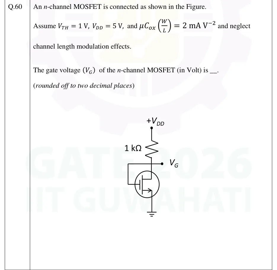
An -channel MOSFET is connected as shown in the Figure.

Assume , , and and neglect channel length modulation effects.

The gate voltage of the -channel MOSFET (in Volt) is ____. (rounded off to two decimal places)

GATE 2026 EC question 60: One n-channel MOSFET, drawn inside a circle, with its drain at the top and its source at the bottom.Tap to open full size
Figure from the GATE 2026 EC paper. It is part of the question.
Figure description

One n-channel MOSFET, drawn inside a circle, with its drain at the top and its source at the bottom. The arrow on the source points away from the channel, towards the source lead, which is the n-channel symbol. The +V_DD rail feeds a 1 kΩ resistor down to a node labelled V_G. That node is the drain, and a wire runs from it to the left and down to the gate, so the gate is tied to the drain (a diode-connected MOSFET). The source goes straight to ground. There are no other components.

Answer and solution
GATE 2026 EC Q.60: answer and solution

GATE 2026 IN Q.22

GATE 2026 · INQ.22 · 1 mark · MCQ

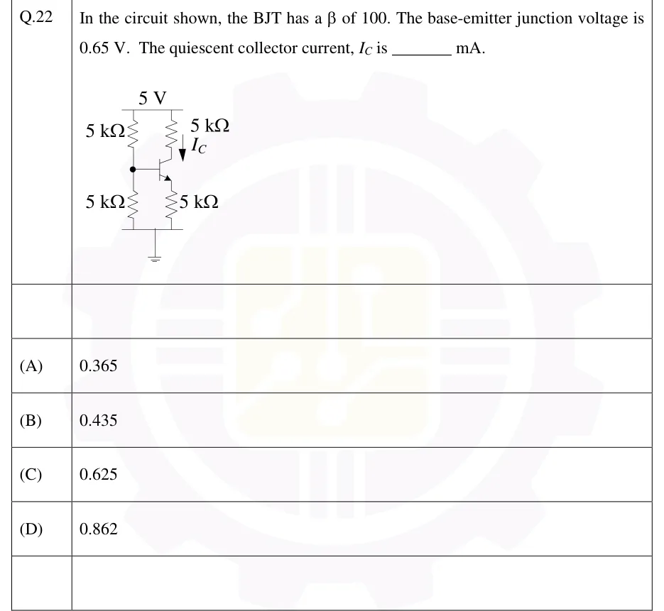
In the circuit shown, the BJT has a of 100. The base-emitter junction voltage is 0.65 V. The quiescent collector current, is _______ mA.

GATE 2026 IN question 22: Voltage-divider bias of an NPN BJT from a single 5 V supply.Tap to open full size
Figure from the GATE 2026 IN paper. It is part of the question.
Figure description

Voltage-divider bias of an NPN BJT from a single 5 V supply. A 5 V rail at the top; ground at the bottom. Left branch: a 5 kΩ resistor from the 5 V rail down to the base node (marked with a dot), and a 5 kΩ resistor from the base node down to ground. The base node connects horizontally to the base of an NPN transistor (emitter arrow pointing outward, downward). Collector (top) connects through a 5 kΩ resistor to the 5 V rail; a downward arrow beside this resistor is labelled I_C (current flowing from the rail into the collector). Emitter (bottom) connects through a 5 kΩ resistor to ground.

  1. (A)

    0.365

  2. (B)

    0.435

  3. (C)

    0.625

  4. (D)

    0.862

Answer and solution
GATE 2026 IN Q.22: answer and solution

GATE 2025 EC Q.22

GATE 2025 · ECQ.22 · 1 mark · MCQ

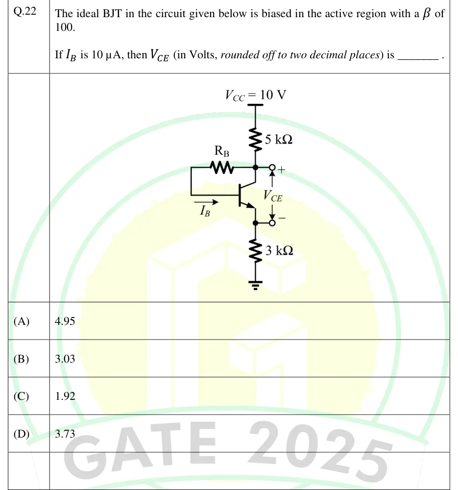
The ideal BJT in the circuit given below is biased in the active region with a of 100.

If is , then (in Volts, rounded off to two decimal places) is ______ .

GATE 2025 EC question 22: Collector-to-base (collector-feedback) bias circuit with an NPN BJT.Tap to open full size
Figure from the GATE 2025 EC paper. It is part of the question.
Figure description

Collector-to-base (collector-feedback) bias circuit with an NPN BJT. Supply V_CC = 10 V at the top connects through a 5 k Ω resistor down to the collector node. From the collector node, resistor R_B (value not given) runs to the left; its left end is wired down to the base of the NPN transistor. An arrow labelled I_B points into the base. The emitter (arrow pointing outward, NPN) connects to the emitter node, which goes through a 3 k Ω resistor to ground. Output terminals: '+' at the collector node and '−' at the emitter node, with V_CE marked between them (collector positive).

  1. (A)

    4.95

  2. (B)

    3.03

  3. (C)

    1.92

  4. (D)

    3.73

Answer and solution
GATE 2025 EC Q.22: answer and solution

GATE 2025 EC Q.47

GATE 2025 · ECQ.47 · 2 marks · MCQ

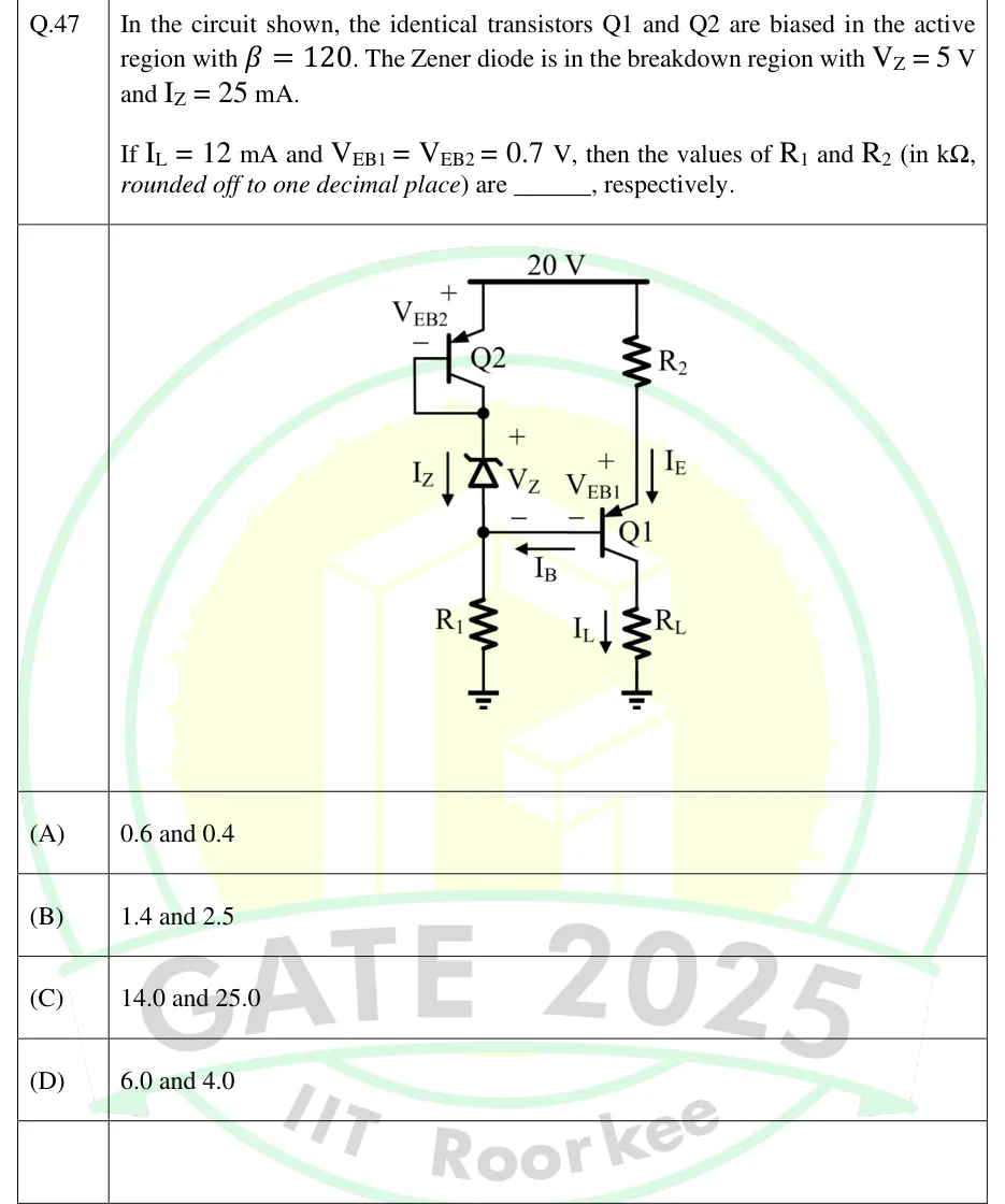
In the circuit shown, the identical transistors Q1 and Q2 are biased in the active region with . The Zener diode is in the breakdown region with and .

If and , then the values of and (in , rounded off to one decimal place) are ______, respectively.

GATE 2025 EC question 47: A +20 V supply rail runs across the top.Tap to open full size
Figure from the GATE 2025 EC paper. It is part of the question.
Figure description

A +20 V supply rail runs across the top. Left branch: PNP transistor Q2 has its emitter connected to the 20 V rail; its base is shorted to its collector (diode-connected), with V_EB2 marked + at the emitter and − at the base. The Q2 collector/base node goes down to the cathode of a Zener diode (Zener drawn pointing upward, cathode at top), with V_Z marked + at the top and − at the bottom, and current I_Z shown flowing downward through it. The Zener anode (bottom node) connects down through resistor R_1 to ground, and also connects to the base of PNP transistor Q1; the base current I_B is shown flowing out of the Q1 base leftward into this node. Right branch: resistor R_2 connects from the 20 V rail down to the emitter of Q1, with current I_E flowing downward through R_2 into the emitter; V_EB1 is marked + at the Q1 emitter and − at its base. The collector of Q1 goes down through load resistor R_L to ground, with I_L flowing downward through R_L.

  1. (A)

    0.6 and 0.4

  2. (B)

    1.4 and 2.5

  3. (C)

    14.0 and 25.0

  4. (D)

    6.0 and 4.0

Answer and solution
GATE 2025 EC Q.47: answer and solution

GATE 2025 IN Q.35

GATE 2025 · INQ.35 · 1 mark · NAT

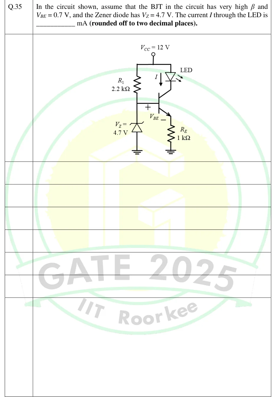
In the circuit shown, assume that the BJT in the circuit has very high and , and the Zener diode has . The current through the LED is ________ mA (rounded off to two decimal places).

GATE 2025 IN question 35: A supply node V_CC = 12 V at the top feeds a horizontal rail.Tap to open full size
Figure from the GATE 2025 IN paper. It is part of the question.
Figure description

A supply node V_CC = 12 V at the top feeds a horizontal rail. On the left, resistor R_1 = 2.2 k Ω runs down from the rail to the base node. From the base node a Zener diode labelled V_Z = 4.7 V goes down to ground, with its cathode at the base node and its anode at ground, so it is reverse-biased. The base node also connects to the base of an NPN BJT, with V_BE marked + at the base and − at the emitter. On the right, an LED runs from the rail (anode) down to the collector (cathode), and the current I is marked flowing downward through it. The emitter (arrow pointing outward) goes through R_E = 1 k Ω to ground.

Answer and solution
GATE 2025 IN Q.35: answer and solution

GATE 2024 EE Q.42

GATE 2024 · EEQ.42 · 2 marks · MCQ

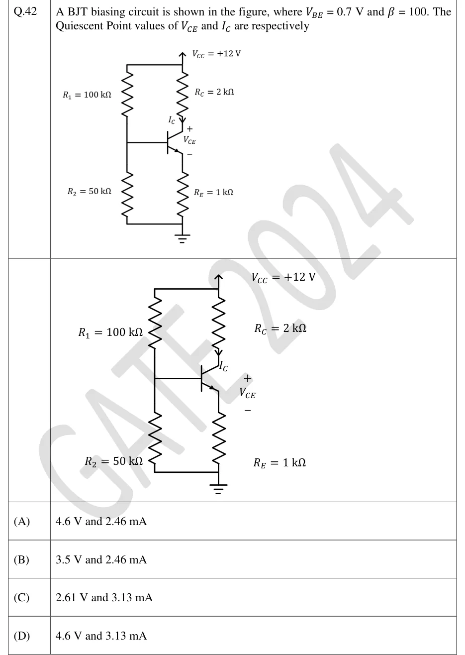
A BJT biasing circuit is shown in the figure, where and . The Quiescent Point values of and are respectively

GATE 2024 EE question 42: Voltage-divider bias circuit with an NPN BJT (emitter arrow pointing outward).Tap to open full size
Figure from the GATE 2024 EE paper. It is part of the question.
Figure description

Voltage-divider bias circuit with an NPN BJT (emitter arrow pointing outward). Supply V_CC = +12 V at the top rail. R_1 = 100 k Ω from the V_CC rail to the base node; R_2 = 50 k Ω from the base node to ground. R_C = 2 k Ω from the V_CC rail to the collector, with current I_C marked by an arrow flowing down into the collector. R_E = 1 k Ω from the emitter to ground. V_CE is marked with + at the collector and − at the emitter. The bottom ends of R_2 and R_E join the common ground. (The printed page shows the same circuit twice, one small copy and one enlarged copy.)

  1. (A)

    4.6 V and 2.46 mA

  2. (B)

    3.5 V and 2.46 mA

  3. (C)

    2.61 V and 3.13 mA

  4. (D)

    4.6 V and 3.13 mA

Answer and solution
GATE 2024 EE Q.42: answer and solution

GATE 2024 IN Q.24

GATE 2024 · INQ.24 · 1 mark · NAT

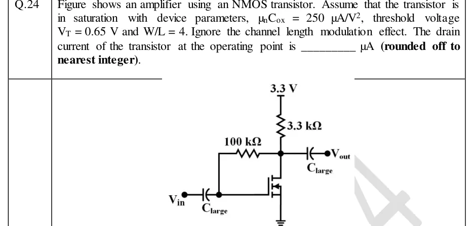
Figure shows an amplifier using an NMOS transistor. Assume that the transistor is in saturation with device parameters, , threshold voltage and . Ignore the channel length modulation effect. The drain current of the transistor at the operating point is ________ A (rounded off to nearest integer).

GATE 2024 IN question 24: Common-source NMOS amplifier with drain-to-gate feedback bias.Tap to open full size
Figure from the GATE 2024 IN paper. It is part of the question.
Figure description

Common-source NMOS amplifier with drain-to-gate feedback bias. A 3.3 V supply connects through a 3.3 kΩ resistor to the drain of an enhancement NMOS transistor, whose source (and body) is grounded. A 100 kΩ resistor connects the drain node directly to the gate node. The input V_in is coupled to the gate through a capacitor C_large. The output V_out is taken from the drain through another capacitor C_large.

Answer and solution
GATE 2024 IN Q.24: answer and solution

GATE 2023 EE Q.59

GATE 2023 · EEQ.59 · 2 marks · NAT

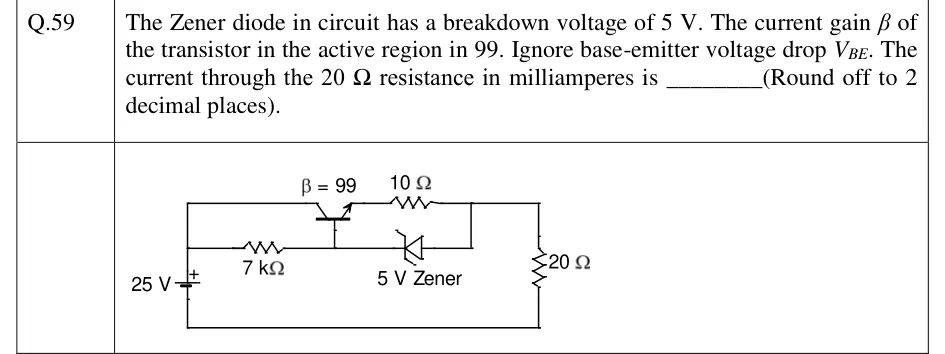
The Zener diode in circuit has a breakdown voltage of 5 V. The current gain of the transistor in the active region in 99. Ignore base-emitter voltage drop . The current through the 20 resistance in milliamperes is ________ (Round off to 2 decimal places).

GATE 2023 EE question 59: A 25 V battery (+ terminal at top) on the left.Tap to open full size
Figure from the GATE 2023 EE paper. It is part of the question.
Figure description

A 25 V battery (+ terminal at top) on the left. From the + terminal a vertical wire rises to a top rail that goes right to the collector of an NPN transistor (β = 99), drawn horizontally: collector on the left, emitter (outward arrow) on the right, base pointing down. The emitter connects through a 10 Ω resistor to a right-hand node (call it L). A second wire leaves the + terminal through a 7 k Ω resistor to the base node B. From B a 5 V Zener diode runs right to node L, with its cathode (bar) at B and its anode (triangle base) at L, so the triangle points toward the base. Node L continues right and down through a 20 Ω resistor to the bottom wire, which returns to the battery's − terminal (ground).

Answer and solution
GATE 2023 EE Q.59: answer and solution

GATE 2022 IN Q.58

GATE 2022 · INQ.58 · 2 marks · NAT

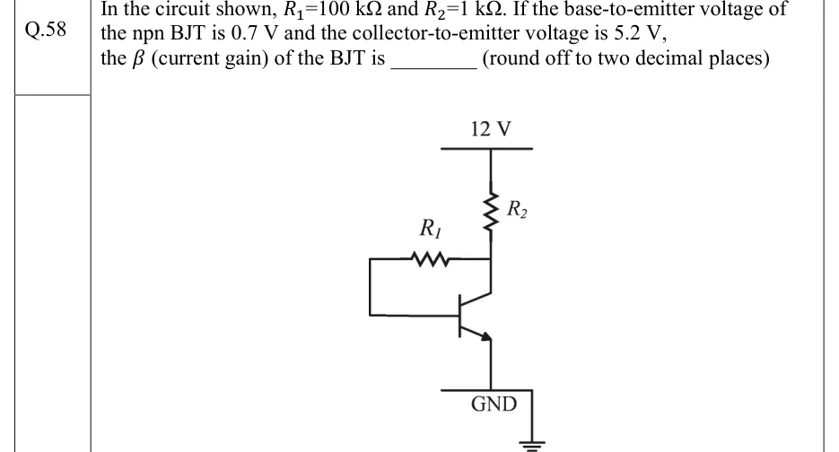
In the circuit shown, and . If the base-to-emitter voltage of the npn BJT is and the collector-to-emitter voltage is , the (current gain) of the BJT is ________ (round off to two decimal places)

GATE 2022 IN question 58: Collector-feedback bias circuit with an npn BJT.Tap to open full size
Figure from the GATE 2022 IN paper. It is part of the question.
Figure description

Collector-feedback bias circuit with an npn BJT. A 12 V supply rail at the top connects through resistor R2 (1 kΩ), drawn vertically, down to the collector node. From the collector node a horizontal resistor R1 (100 kΩ) runs to the left. Its left end drops down and returns right into the base of the transistor, so R1 connects collector to base. The emitter (arrow pointing outward, npn) goes straight down to the GND line, which is tied to the earth symbol. No emitter resistor and no input source.

Answer and solution
GATE 2022 IN Q.58: answer and solution

GATE 2018 EC Q.43

GATE 2018 · ECQ.43 · 2 marks · NAT

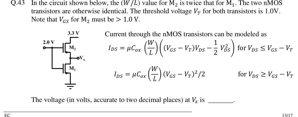
In the circuit shown below, the value for is twice that for . The two nMOS transistors are otherwise identical. The threshold voltage for both transistors is 1.0V. Note that for must be .

Current through the nMOS transistors can be modeled as

The voltage (in volts, accurate to two decimal places) at is ______.

GATE 2018 EC question 43: Two enhancement nMOS transistors stacked in series between a 3.3 V supply and ground.Tap to open full size
Figure from the GATE 2018 EC paper. It is part of the question.
Figure description

Two enhancement nMOS transistors stacked in series between a 3.3 V supply and ground. Upper transistor M2: drain connected to the 3.3 V rail, source connected to the output node labelled V_x (open-circle terminal to the right), gate connected to an input node held at 2.0 V (open-circle terminal on the left labelled 2.0 V). Lower transistor M1: drain connected to node V_x, source connected to ground, gate also connected to the same 2.0 V node (a vertical wire from the 2.0 V node runs down to M1's gate, so both gates are tied to 2.0 V). Source terminals carry the nMOS arrow; no separate body terminal is drawn (body effect not considered).

Answer and solution
GATE 2018 EC Q.43: answer and solution

GATE 2018 EE Q.41

GATE 2018 · EEQ.41 · 2 marks · NAT

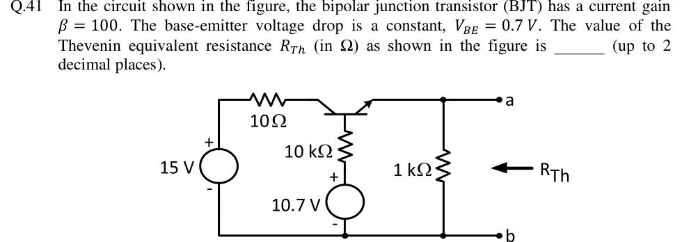
In the circuit shown in the figure, the bipolar junction transistor (BJT) has a current gain . The base-emitter voltage drop is a constant, . The value of the Thevenin equivalent resistance (in ) as shown in the figure is ______ (up to 2 decimal places).

GATE 2018 EE question 41: An npn BJT is drawn on its side along the top wire.Tap to open full size
Figure from the GATE 2018 EE paper. It is part of the question.
Figure description

An npn BJT is drawn on its side along the top wire. Its collector (left lead) goes through a 10 Ω resistor to the + terminal of a 15 V DC source. The source's − terminal is on the bottom (ground) wire. The emitter (right lead, arrow pointing outward, so npn) connects to node a. The base lead points down and goes through a 10 kΩ resistor to the + terminal of a 10.7 V DC source, whose − terminal is on the ground wire. A 1 kΩ resistor runs from node a to the ground wire, which is node b. An arrow marked R_Th points into terminals a–b from the right.

Answer and solution
GATE 2018 EE Q.41: answer and solution

GATE 2018 IN Q.15

GATE 2018 · INQ.15 · 1 mark · NAT

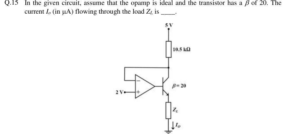
Q.15 In the given circuit, assume that the opamp is ideal and the transistor has a of 20. The current (in A) flowing through the load is ______.

GATE 2018 IN question 15: An op-amp drives an NPN transistor.Tap to open full size
Figure from the GATE 2018 IN paper. It is part of the question.
Figure description

An op-amp drives an NPN transistor. The non-inverting (+) input of the op-amp is tied to a fixed 2 V source. The op-amp output connects to the base of the NPN transistor (labelled β = 20). The collector connects through a 10.5 kΩ resistor up to a +5 V supply. A wire from the collector node (the junction of the 10.5 kΩ resistor and the collector) runs back to the inverting (−) input of the op-amp. The emitter connects through a load Z_L (value not given) to ground. The load current I_o is marked by a downward arrow through Z_L towards ground.

Answer and solution
GATE 2018 IN Q.15: answer and solution

PRACTICE

6 questions to test yourself

PRACTICE 11 mark · NAT

An npn transistor with has its emitter grounded and a collector resistor kΩ to V. Its base is driven from a 5 V source through kΩ. Take V in the active region, and V and V in saturation. The collector current, in mA, is ______.

Answer and solution

Answer: (accepted range )

  1. Assume active: mA, so mA.

  2. Then V, below . The active assumption fails.

  3. Assume saturation: mA and mA.

  4. Check: , so the transistor is saturated and mA.

PRACTICE 22 marks · NAT

An enhancement NMOS with V, mA/V² and is biased from V by a gate divider: MΩ from to the gate and MΩ from the gate to ground. kΩ is connected from to the drain and kΩ from the source to ground. The source is tied to the body. In saturation, . The drain current, in mA, is ______ (to two decimal places).

Answer and solution

Answer: (accepted range )

  1. V, since .

  2. Bias line (with in mA): . In saturation , so gives , i.e. .

  3. V. The other root, V, gives V, below , so it is rejected.

  4. mA, which is 0.85 mA to two decimal places.

  5. Check: V and V, so V, well above V. The device is saturated.

PRACTICE 32 marks · NAT

An npn transistor is biased from V by a divider, kΩ from to the base and kΩ from the base to ground, with kΩ and kΩ. Take V in the active region and neglect leakage. If the transistor is replaced by one with instead of , the percentage increase in the collector current is ______ (to one decimal place).

Answer and solution

Answer: (accepted range )

  1. Thévenin equivalent: V and kΩ.

  2. : mA mA.

  3. : mA mA. Then V, so the transistor is still active.

  4. Increase , i.e. 4.3%.

  5. Cross-check with the large-change formula: , A, and mA. In fixed bias, doubling would double (a 100% increase).

PRACTICE 41 mark · MCQ

An enhancement PMOS transistor has threshold voltage V and . In a circuit its terminal voltages are V, V and V. The region of operation of the transistor is

  1. (A)

    cut-off

  2. (B)

    triode (linear)

  3. (C)

    saturation

  4. (D)

    impossible to determine without the value of

Answer and solution

Answer: (C)

  1. V, which exceeds V, so the device is on.

  2. Saturation needs V.

  3. V, which is at least 0.9 V, so the device is in saturation.

  4. The region depends only on the terminal voltages; scales the current and plays no part in the test.

PRACTICE 52 marks · MSQ

Which of the following statements about DC biasing are correct? Assume the constant-drop BJT model and a square-law MOSFET with ; leakage is included only where a stability factor is involved.

  1. (A)

    In fixed bias (base resistor to , no emitter resistor), the stability factor equals .

  2. (B)

    In voltage-divider bias with held fixed, increasing decreases the stability factor .

  3. (C)

    An enhancement NMOS with its gate tied to its drain operates in the triode region whenever .

  4. (D)

    For a BJT whose collector-emitter voltage is (taking ), a Q-point with means that a small rise in reduces the transistor's dissipation .

Answer and solution

Answer: (A), (B), (D)

  1. A is correct. In fixed bias does not depend on , so and .

  2. B is correct. , and its derivative with respect to has numerator , so falls as grows.

  3. C is wrong. With the gate tied to the drain, , so the device is always in saturation, never triode.

  4. D is correct. , which is negative when .

PRACTICE 62 marks · MCQ

In a collector-to-base bias circuit, an npn transistor (, V) has kΩ from V to the collector, kΩ from the collector to the base, and its emitter grounded. The collector-emitter voltage is closest to

  1. (A)

    5.33 V

  2. (B)

    5.37 V

  3. (C)

    0.70 V

  4. (D)

    0.20 V

Answer and solution

Answer: (A)

  1. KVL from through and to the base: .

  2. A, so mA and mA.

  3. V.

  4. B comes from finding correctly but then charging with alone: V. C comes from treating the circuit as fixed bias ( returned to ): A, mA, V. D is impossible: , so this circuit cannot saturate.

OFFICIAL GATE 2027 SYLLABUS WORDING

Copied from the GATE 2027 syllabus; see all 2027 syllabi.

GATE EC

BJT and MOSFET Amplifiers: Biasing

GATE EE

Amplifiers: biasing

GATE IN

BJT and MOSFET circuits, biasing, power dissipation, DC analysis

Preparing in Kolkata? IAE Academy's course for GATE ECE, GATE EE or GATE IN.