GATE 2026 EC Q.42
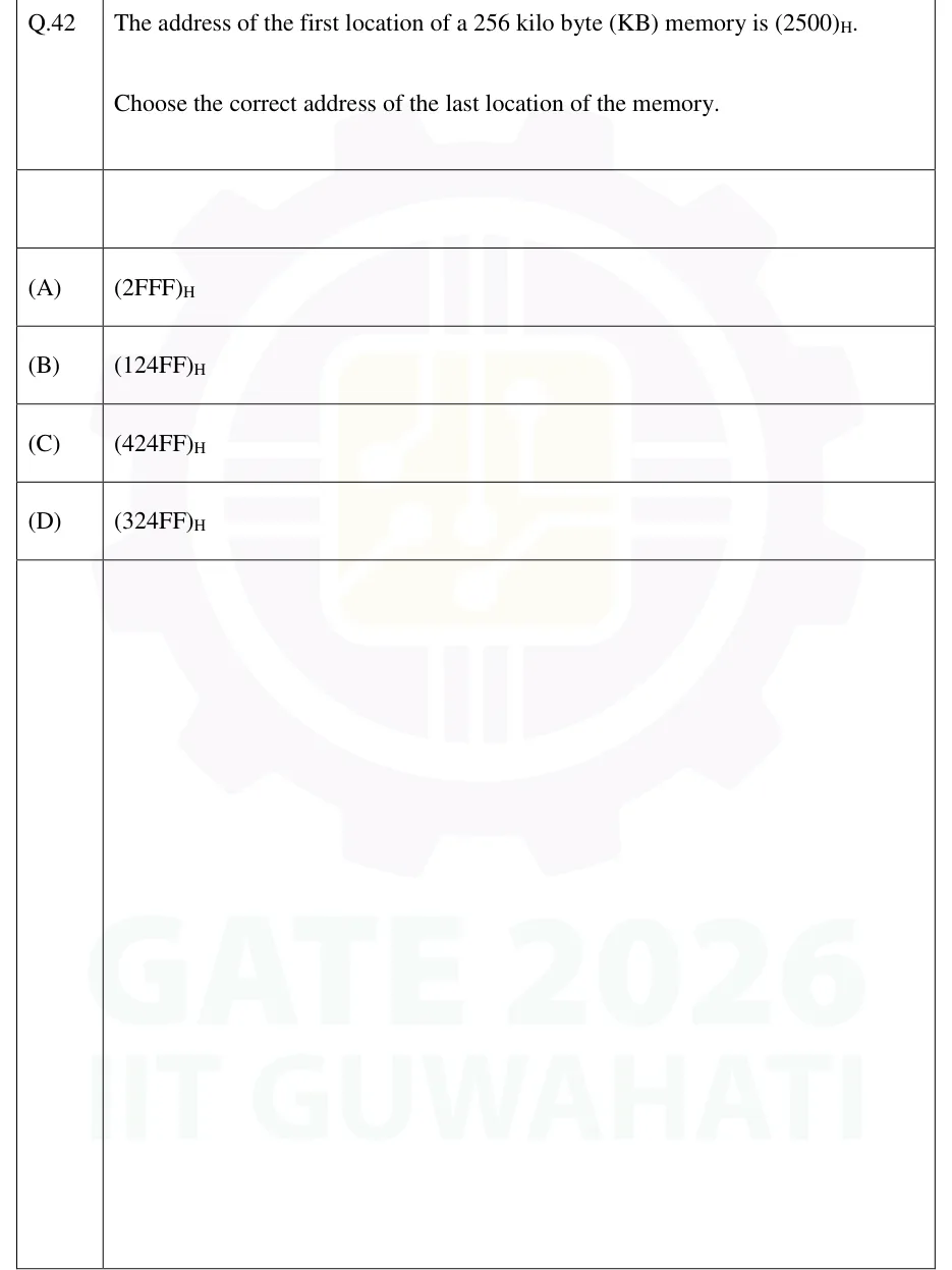
The address of the first location of a 256 kilo byte (KB) memory is .
Choose the correct address of the last location of the memory.
- (A)
- (B)
- (C)
- (D)

IN THE EC AND IN SYLLABUS
Memories, computer organisation, microprocessors and embedded systems
This topic covers how semiconductor memories (ROM, SRAM, DRAM) store bits and are wired into an address map, how a processor encodes instructions, locates operands and sequences its datapath through a control unit, and how pipelining raises throughput; for IN it extends to microprocessors, microcontrollers, memory and I/O interfacing, embedded programming and data acquisition. Solving questions here rests on a small set of exact counting results (chip counts and address ranges, effective addresses, pipeline speed-up with stalls, 8085 T-state delays, microinstruction widths) and on applying the stated convention (PC value after fetch, latch delay, forwarding, resolution definition) correctly.
9 previous-year questions · 9 solved · 5 practice questions
Semiconductor memory is classified by what happens at power-off. Volatile memory (SRAM, DRAM) loses its contents; non-volatile memory (the ROM family) keeps them. Random access means every location is reached in the same time whatever its address. SRAM and DRAM are read/write random-access memories; ROMs are random-access too, but in common usage RAM means read/write memory.
Conventions used throughout these notes: positive logic; an overline marks an active-low signal (for example selects a chip when it is 0) and also the complement of a bit; address and data bits are numbered MSB first, down to on a 16-bit bus; signed numbers are 2's complement.
The ROM family
Type | Programmed | Erased | Remarks |
|---|---|---|---|
Mask ROM | By the manufacturer, through a fabrication mask | Cannot be erased | Economical only in large volumes |
PROM | Once, by the user (fuses blown or antifuses formed) | Cannot be erased | One-time programmable (OTP) |
EPROM | Electrically, by trapping charge on a floating gate | Ultraviolet light through a quartz window; whole chip, out of circuit | Floating-gate transistor |
EEPROM | Electrically | Electrically, byte by byte, in circuit | Limited number of write cycles; slow writes |
Flash | Electrically | Electrically, one block (sector) at a time | Floating-gate; denser than EEPROM; used for firmware |
ROM AS A COMBINATIONAL CIRCUIT
A ROM with n address inputs and m data outputs stores a complete truth table, so it implements any m Boolean functions of the same n variables: each address is one input combination and each word holds the m outputs for it. Example: a squarer for a 4-bit unsigned input (largest output , which needs 8 bits) needs a ROM, 128 bits.
SRAM: the 6T cell. Two cross-coupled CMOS inverters (four transistors) form a latch holding and . Two access transistors, gated by the word line WL, connect and to the bit lines BL and .
Read: both bit lines are precharged high, WL is raised, and the side storing 0 pulls its bit line slightly low; a differential sense amplifier resolves the bit. The stored value is not lost. Write: write drivers force BL and to opposite levels, overpowering the latch. Hold: with WL low the latch keeps its state for as long as power is applied. No refresh is needed; that is what static means.
DRAM: the 1T1C cell. One access transistor connects a storage capacitor to the bit line when the word line is high; the bit is the charge on .
Read: the bit line is precharged (commonly to ), the word line is raised, and charge sharing between and the much larger bit-line capacitance shifts the bit line by a small , which a sense amplifier amplifies. Charge sharing destroys the stored level, so the sense amplifier writes the value back (restore): a DRAM read is destructive.
Leakage: the stored charge leaks away, so every row must be read and restored (refreshed) once in every refresh period , whether it is accessed or not. Opening a row refreshes every cell in that row together.
Addressing: to save pins, the row address and then the column address are sent on the same pins, latched by and .
Cycle time: after each access the row must be restored and the bit lines precharged again, so a DRAM's cycle time (the minimum interval between successive accesses) is longer than its access time.
SRAM versus DRAM
Property | SRAM | DRAM |
|---|---|---|
Cell | 6 transistors (latch + 2 access) | 1 transistor + 1 capacitor |
Bit stored as | State of a bistable latch | Charge on a capacitor |
Refresh | Not needed while powered | Needed periodically |
Read | Non-destructive | Destructive; value written back |
Speed | Faster | Slower |
Density and cost per bit | Lower density, higher cost | Higher density, lower cost |
Address pins | Full address at once | Row and column multiplexed |
Volatile | Yes | Yes |
Typical use | Cache memory, register files | Main memory |
DRAM READ: CHARGE-SHARING SIGNAL
= bit-line precharge voltage, = voltage on . Positive reads as 1, negative as 0; it is small because .
DRAM DISTRIBUTED-REFRESH INTERVAL
R = number of rows (one refresh operation per row); = period within which every row must be refreshed. Spread evenly, one row is refreshed every .
DRAM REFRESH OVERHEAD
= duration of one row-refresh cycle. The same fraction applies to burst refresh (all rows back to back) and to distributed refresh.
DRAM ADDRESS PINS WITH ROW/COLUMN MULTIPLEXING
A DRAM with addressable locations arranged as rows by columns; for a square array .
WORKED EXAMPLE · WORKED EXAMPLE: REFRESH BUDGET
A DRAM has 8192 rows. Every row must be refreshed once every 64 ms, and one row refresh takes 50 ns. Find (a) the interval between row refreshes if refresh is spread evenly, and (b) the percentage of time the memory is busy refreshing.
Rows: .
(a) .
(b) Time spent refreshing per period .
Fraction .
Answer: (a) ; (b) .
EXAM TIP
Refresh is counted per row, not per bit: a DRAM with 8192 rows needs 8192 refresh operations per period however many columns it has. Static (SRAM) means no refresh; it does not mean non-volatile, since SRAM and DRAM both lose data at power-off. EPROM is erased by ultraviolet light and EEPROM electrically; a statement that swaps the two is false.
A chip organised as holds words of bits. It has address lines , data lines, and active-low controls: chip select , output enable (read) and write enable . In memory sizes and ; a size written with B (such as 16 KB) is in bytes, while a size written as is W words of m bits.
CHIP CAPACITY
n = number of address lines, m = number of data lines (word size). Divide by 8 for bytes.
ADDRESS LINES FOR W WORDS
Address lines depend only on the number of words; data lines depend only on the word size.
Width (word-size) expansion: chips placed side by side share every address line and the same chip select; each drives its own slice of the data bus (two chips make ).
Depth (word-count) expansion: banks share the low address lines and the data bus; a decoder driven by the higher address lines enables exactly one bank at a time. A general design uses both.
NUMBER OF CHIPS
Target memory (words bits) built from chips: banks, each chips wide. If either ratio is not a whole number, round it up.
BANK-SELECT DECODER
For a contiguous block with a power of 2: the k decoder inputs are the address lines immediately above the chip's own lines, and each decoder output drives the of one bank.
ADDRESS RANGE OF A BLOCK
Size in addressable units: 1K = 400H, 2K = 800H, 4K = 1000H, 8K = 2000H, 16K = 4000H, 32K = 8000H.
Finding the address range of a chip
Chip lines: , connected to .
Select lines: the remaining upper lines ( on a 16-bit bus) drive gates or a decoder that asserts .
First address: the select pattern on the upper lines with every chip line 0. Last address: the same select pattern with every chip line 1.
Group the 16 bits in fours starting from and convert each group to hex.
Check: must equal the chip size.
Full (absolute) decoding uses every upper address line, so each location has exactly one address. Partial decoding leaves some upper lines unconnected to save logic; each location then responds at several addresses (fold-back or mirror images). Partial decoding is acceptable only if no image overlaps another device.
IMAGES UNDER PARTIAL DECODING
u = number of address lines that are neither chip lines nor used in the select logic.
WORKED EXAMPLE · WORKED EXAMPLE: RAM FROM SMALLER CHIPS
An 8085 system (address bus ) needs 16 KB of RAM at consecutive addresses starting from 8000H, built from chips with full decoding. Find the number of chips, the decoder arrangement, and the address range of each bank.
Target , chip : chips, in 4 banks of 2 (one chip supplies , the other ).
Each chip has address lines: .
Four banks need a 2-to-4 decoder on . Throughout 8000H to BFFFH, , so and enable the decoder (full decoding uses every line).
Bank 0: , 8000H to 8FFFH. Bank 1: , 9000H to 9FFFH. Bank 2: , A000H to AFFFH. Bank 3: , B000H to BFFFH.
Check: each range spans 1000H = 4096 addresses, and 8000H + 4000H − 1 = BFFFH.
Answer: 8 chips in 4 banks; a 2-to-4 decoder on , enabled by , ; banks at 8000H–8FFFH, 9000H–9FFFH, A000H–AFFFH and B000H–BFFFH.
EXAM TIP
Two traps in address-range questions: reading the select bits in the wrong order (the pattern is B, not D), and mixing words with bytes. Under partial decoding, count the unused lines and expect images of each location; a question may ask for any one of them.
A machine instruction is a binary word with an opcode field (the operation) and operand fields (register numbers, memory addresses or constants). Instruction groups are data transfer, arithmetic and logic, branch and control, and input/output. The number of explicit addresses gives the instruction format: more addresses per instruction means fewer instructions per program but longer instructions.
Instruction formats
Format | Code for X = A + B | Remarks |
|---|---|---|
3-address | ADD X, A, B | Destination and both sources explicit |
2-address | MOV X, A ; ADD X, B | Destination is also a source |
1-address | LOAD A ; ADD B ; STORE X | Accumulator implied |
0-address | PUSH A ; PUSH B ; ADD ; POP X | Stack machine: operands on the top of the stack |
OPCODE FIELD WIDTH
distinct operations coded in one fixed-width opcode field.
INSTRUCTION LENGTH
p opcode bits, r register fields for registers, and a bits of address, displacement or immediate fields (a memory-address field for addressable units needs a bits).
EXPANDING OPCODE
Fixed-length instructions in two classes. The class with more operands has a p-bit opcode and instructions, using of the patterns; each unused pattern is extended by the f bits of the operand field that the class with fewer operands does not need, giving at most instructions in that class.
The addressing mode tells the processor how to find the operand or its effective address (EA). Notation: A = the address or displacement field of the instruction, R = a register, M[x] = contents of memory location x. The memory-reference column counts the accesses needed to obtain the operand after the instruction itself has been fetched.
Addressing modes
Mode | Operand or EA | Memory references for the operand | Typical use |
|---|---|---|---|
Immediate | Operand = A | 0 | Constants |
Direct (absolute) | EA = A | 1 | Fixed variables |
Memory indirect | EA = M[A] | 2 | Pointers held in memory |
Register | Operand = R | 0 | Fast temporaries |
Register indirect | EA = R | 1 | Pointers held in registers |
Indexed | EA = A + index register | 1 | Arrays: A is the base address, the register holds the index |
Base register (displacement) | EA = base register + A | 1 | Relocatable programs and data |
PC-relative | EA = PC of next instruction + A, with A in 2's complement | 1 for a data operand; 0 to form a branch target | Branches, position-independent code |
Auto-increment / auto-decrement | Convention used here: post-increment EA = R, then R ← R + s; pre-decrement R ← R − s, then EA = R (s = operand size in addressable units) | 1 | Stepping through arrays and stacks |
Implied | Operand fixed by the opcode | 0 | For example, complement the accumulator |
PC-RELATIVE BRANCH TARGET
= address of the instruction after the branch (the PC has already advanced during fetch), unless a question states that the offset is added to the branch's own address; d = q-bit 2's-complement offset in bytes. If the offset counts words or instructions, multiply d by their size first.
WORKED EXAMPLE · WORKED EXAMPLE: EXPANDING OPCODE
A processor has fixed 16-bit instructions and 64 general-purpose registers. It has 14 two-register instructions (opcode, register, register). (a) What is the largest number of one-register instructions it can also have? (b) If exactly 120 one-register instructions are implemented, how many zero-register instructions are possible at most?
Register field: bits.
Two-register format: bits, giving patterns; 14 are used, 2 are free.
(a) Each free pattern extends by the 6 bits of the unused second register field: .
(b) Of the 128 one-register patterns, are free; each extends by the remaining 6-bit register field: .
Answer: (a) 128; (b) 512.
WORKED EXAMPLE · WORKED EXAMPLE: PC-RELATIVE OFFSET
A 2-byte conditional branch is stored at 3000H–3001H in a byte-addressable machine. Its second byte is an 8-bit 2's-complement offset added to the PC after fetch. The branch target is 2FF0H. Find the offset byte and the range of targets this instruction can reach.
After both bytes are fetched, = 3002H.
= 2FF0H − 3002H = −12H = −18 (decimal).
8-bit 2's complement of −18: = EEH.
runs from −128 to +127, that is −80H to +7FH, so targets run from 3002H − 80H = 2F82H to 3002H + 7FH = 3081H.
Answer: Offset byte EEH; reachable targets 2F82H to 3081H.
EXAM TIP
PC-relative offsets are measured from the next instruction, not from the branch itself, unless the question says otherwise. Count operand memory references carefully: memory indirect needs two (pointer, then operand), register indirect one, register and immediate none. Indexed and base-register modes compute the same kind of sum; they differ in which part is fixed in the instruction (the base address in indexed mode, the displacement in base-register mode).
The ALU is a combinational block: an adder with input conditioning performs add, subtract (as ), increment, decrement and compare; a logic unit performs AND, OR, XOR and NOT; a shifter performs shifts and rotates. A function-select code from the control unit chooses the operation. The ALU also produces status flags: carry C (carry or borrow out of the MSB, meaningful for unsigned numbers), zero Z, sign S (the MSB of the result), overflow V (signed overflow) and parity P.
2'S-COMPLEMENT SUBTRACTION IN THE ADDER
= bitwise complement of B; the +1 enters as the adder's carry-in. The adder's carry-out is then 1 when (unsigned), that is, it is the complement of the borrow; some processors, the 8085 among them, store the borrow in the carry flag instead.
SIGNED OVERFLOW FLAG
n-bit addition: = carry into the MSB (bit n−1), = carry out of the MSB. Equivalently, an addition overflows when both operands have the same sign and the result has the opposite sign, and adding operands of opposite sign never overflows; a subtraction overflows when A and B have opposite signs and the result's sign differs from A's.
RANGE OF N-BIT 2'S-COMPLEMENT NUMBERS
An 8-bit signed value runs from −128 to +127.
The datapath is the ALU together with the registers and buses that feed it: program counter PC, instruction register IR, memory address register MAR, memory data register MDR, the general-purpose registers and the flag register. The control unit issues, in every clock period, the control signals (register load enables, bus and multiplexer selects, ALU function, memory read/write) that make the datapath perform one step of the instruction cycle. On a single internal bus only one register can drive the bus in a step, which is why a fetch takes several steps.
Instruction cycle in register-transfer steps (one-word instruction, word-addressed memory)
: MAR ← PC.
: MDR ← M[MAR]; PC ← PC + 1.
: IR ← MDR.
Decode the opcode held in IR.
Operand fetch: form the effective address as the addressing mode dictates and read the operand (one more memory cycle per memory reference).
Execute: the ALU operates and the flags are updated.
Write back the result to a register or memory, check for a pending interrupt, and start the next fetch.
Hardwired versus microprogrammed control
Aspect | Hardwired control | Microprogrammed control |
|---|---|---|
How control signals are produced | Combinational logic driven by the opcode, a step counter and the flags (a finite-state machine) | Microinstructions read from a control memory, one per step, addressed by a control address register |
Speed | Faster | Slower: a control-memory read in every step |
Changing or adding instructions | Redesign the logic | Rewrite the control-memory contents |
Suits | Small, regular instruction sets (RISC) | Large, complex instruction sets (CISC) |
Design effort for a complex set | High | Lower and systematic |
Horizontal microinstructions have one bit per control signal: wide words, no decoding, and any combination of signals can be active together. Vertical microinstructions encode each group of mutually exclusive signals (signals never active in the same step) into a short field that is decoded: a narrower control memory, at the cost of decoding delay and less parallelism. In the format used in these notes, each microinstruction also carries sequencing information: a condition-select field (which flag to test) and a next-address field (the branch target in control memory).
HORIZONTAL MICROINSTRUCTION WIDTH
control signals (one bit each); c = condition-select bits ; a = next-address bits .
VERTICAL (ENCODED) FIELD WIDTH
A group of k mutually exclusive signals; the extra code means none of them is active. If a question states that one signal of the group is always active, use .
CONTROL-MEMORY SIZE
In bits.
PROCESSOR EXECUTION TIME
IC = instructions executed, CPI = average clock cycles per instruction. Speed comparisons use the ratio of execution times. MIPS rating .
WORKED EXAMPLE · WORKED EXAMPLE: CONTROL-MEMORY SIZE
A microprogrammed control unit drives 30 control signals that fall into three groups of mutually exclusive signals, of sizes 3, 10 and 17. The control memory holds 256 microinstructions. Each microinstruction selects one of 4 status flags or an unconditional branch, and has a next-address field. Find the control-memory size in bits for (a) horizontal and (b) vertical encoding of the control signals.
Next-address field: bits.
Condition select: 4 flags + unconditional = 5 choices, so bits.
(a) Horizontal width bits; size bits.
(b) Vertical fields: bits (each group needs a none-active code).
Vertical width bits; size bits.
Answer: (a) 10496 bits; (b) 5632 bits.
EXAM TIP
Carry and overflow are different flags: 70H + 70H in 8 bits gives E0H with carry 0 but overflow 1, because 112 + 112 exceeds +127. Carry judges unsigned results, overflow judges signed ones. The 8085's five documented flags (S, Z, AC, P, CY) include no overflow flag, and after SUB or CMP its CY flag is a borrow: CY = 1 means the subtrahend was larger (unsigned).
Pipelining splits instruction processing into stages separated by latches (pipeline registers), so instructions are in progress at once, each in a different stage. The classic 5-stage pipeline is IF (instruction fetch), ID (decode and register read), EX (ALU operation or address calculation), MEM (data-memory access) and WB (write back to the register file). All stages share one clock, so its period is set by the slowest stage plus the latch delay. Pipelining does not make one instruction faster; it raises the rate at which instructions complete.
PIPELINE CLOCK PERIOD
= delay of stage i, = inter-stage register delay.
TIME FOR N INSTRUCTIONS ON A K-STAGE PIPELINE
k cycles for the first instruction to pass through, then one completion per cycle; no stalls.
SPEED-UP OVER THE NON-PIPELINED PROCESSOR
= non-pipelined time per instruction; unless stated, the sum of the stage delays without latch delay. As , .
IDEAL SPEED-UP (BALANCED STAGES)
Holds when : equal stage delays, no latch overhead, no stalls. With taken as the sum of the stage delays, the speed-up of a k-stage pipeline never exceeds k.
EFFICIENCY AND THROUGHPUT
Efficiency is defined here as S/k. For balanced stages with no latch delay and no stalls it equals , the fraction of stage slots doing useful work; some questions define efficiency directly as that fraction, so check which is meant. Throughput is in instructions per unit time.
CPI WITH STALLS
Sum each hazard's frequency times its stall cycles. For branches the term is , with p = fraction of branches that pay the penalty (taken, or mispredicted) and b = penalty in cycles.
TIME FOR N INSTRUCTIONS WITH STALLS
= total stall (bubble) cycles in the run, for an in-order pipeline in which each stall cycle delays every later instruction by one cycle.
SPEED-UP WITH STALLS (LONG PROGRAMS)
The first form is general; the second assumes .
BRANCH PENALTY (STALL UNTIL RESOLVED)
s = number of the stage (IF = 1) at the end of which both the branch outcome and the target are known: resolved in ID gives 1 bubble, in EX 2, in MEM 3.
Pipeline hazards
Hazard | Cause | Remedies |
|---|---|---|
Structural | Two instructions need the same hardware in the same cycle, for example one memory port wanted by IF and MEM | Duplicate the resource (separate instruction and data memories), or stall |
Data: RAW (true dependence) | An instruction reads a register before an earlier instruction has written it | Forwarding (bypassing), stalls (bubbles), compiler reordering or NOPs |
Data: WAR and WAW (name dependences) | A later instruction writes a register that an earlier one still has to read (WAR) or write (WAW) | Register renaming; in a simple in-order 5-stage pipeline these dependences cause no hazard, because every register read happens in ID and every write in WB, in program order |
Control | The next fetch address is unknown until a branch resolves | Stall or flush, predict not-taken or taken, delayed branch, resolve the branch in an earlier stage |
Counting stalls in the classic 5-stage pipeline (state the question's conventions first)
Draw the space-time chart: without stalls, instruction i enters IF in cycle i.
RAW on the immediately preceding ALU instruction, with full forwarding: 0 stalls (the EX result is forwarded to the next instruction's EX).
RAW on the immediately preceding load, with forwarding: 1 stall (the loaded value exists only at the end of MEM).
RAW without forwarding, register file written in the first half of a cycle and read in the second half: 2 stalls for an immediately following consumer (its ID must line up with the producer's WB); 3 stalls if the register file cannot write and read in the same cycle.
A consumer two instructions after the producer needs one stall fewer, and so on, never fewer than zero.
A branch resolved at the end of stage s costs bubbles under stall-until-resolved; with predict-not-taken the penalty is paid only when the branch is taken.
WORKED EXAMPLE · WORKED EXAMPLE: SPEED-UP, THROUGHPUT AND LOAD-USE STALLS
A processor is split into a 5-stage pipeline with stage delays 160, 220, 200, 240 and 180 ps; each pipeline latch adds 10 ps. (a) Find the speed-up over the non-pipelined processor for 1000 instructions with no stalls. (b) Find the limiting speed-up and throughput for very long programs. (c) Now 20% of instructions are loads, and 40% of loads are immediately followed by a dependent instruction, costing 1 stall each (forwarding present, no other stalls). Find the speed-up for very long programs.
Non-pipelined time per instruction (no latches): ps.
Clock: ps.
(a) Non-pipelined: ps. Pipelined: ps. .
(b) ; throughput instructions per second.
(c) Stalls per instruction , so and the average time per instruction is ps. .
Answer: (a) ; (b) 4, and instructions per second; (c) .
EXAM TIP
Read the conventions before calculating: whether the non-pipelined machine includes latch delay (normally not), whether the register file writes in the first half and reads in the second half of a cycle, whether forwarding exists, and in which stage branches resolve. With unequal stages the limiting speed-up is , not k. The latency of one instruction in the pipeline is ; with the sum of the stage delays it is never shorter than , and it is longer whenever the stages are unequal or the latches add delay.
Microprocessor versus microcontroller
Aspect | Microprocessor (for example 8085) | Microcontroller (for example 8051) |
|---|---|---|
On the chip | CPU only: ALU, registers, control, bus interface | CPU plus program memory, data RAM, timers, serial port and parallel I/O ports (often ADC and PWM too) |
External chips needed | Memory, I/O ports, timers | Few or none |
Memory spaces | One space shared by program and data (8085) | Separate program and data spaces (8051) |
Instruction-set emphasis | Data movement and arithmetic | Adds bit-level operations for control |
Typical role | General-purpose computing | Dedicated control inside a product |
The 8085 at a glance. 8-bit data bus and 16-bit address bus (64 KB memory space). The low address byte and the data share pins ; an external latch strobed by ALE in the first T-state of each machine cycle holds . Registers: accumulator A; general-purpose B, C, D, E, H, L, usable as the 16-bit pairs BC, DE, HL (HL is the memory pointer M); 16-bit stack pointer SP and program counter PC; the flag register with S (), Z (), AC (), P () and CY (). Multi-byte values are stored low byte first: in a 3-byte instruction the second byte is the low-order byte of the address or data (LDA 2050H is stored as 3A, 50, 20), and a 16-bit word in memory has its low byte at the lower address. The stack grows toward lower addresses and SP points to the last byte stored: PUSH rp stores the high-order register at SP − 1 and the low-order register at SP − 2, then SP ← SP − 2; POP reverses this and adds 2 to SP; CALL pushes the return address (the address of the instruction after the CALL). Control and status pins include , , , ALE, READY (inserts wait states for slow devices) and HOLD/HLDA (for DMA).
An instruction takes one or more machine cycles: opcode fetch takes 4 T-states (6 for some, such as INX, DCX, PUSH and CALL); memory read, memory write, I/O read and I/O write take 3 T-states each. One T-state is one clock period.
8085 timing of common instructions
Instruction | Bytes | T-states |
|---|---|---|
MOV r1, r2 | 1 | 4 |
MOV r, M / MOV M, r | 1 | 7 |
MVI r, data | 2 | 7 |
LXI rp, data16 | 3 | 10 |
LDA addr / STA addr | 3 | 13 |
ADD r, SUB r, INR r, DCR r | 1 | 4 |
INX rp / DCX rp | 1 | 6 |
JMP addr | 3 | 10 |
JNZ, JZ, JC, JNC addr | 3 | 10 if taken, 7 if not |
CALL addr | 3 | 18 |
RET | 1 | 10 |
PUSH rp / POP rp | 1 | 12 / 10 |
IN port / OUT port | 2 | 10 |
8085 CLOCK AND T-STATE
A 6 MHz crystal gives a 3 MHz clock and a T-state of 333.3 ns. Execution time = total T-states × T.
8085 DELAY LOOP, 8-BIT COUNTER
MVI C, N (7); LOOP: DCR C (4); JNZ LOOP (10 when taken, 7 on the final pass). N = 1 to 255; loading 00H gives 256 passes (use N = 256), because DCR takes 00H to FFH.
8085 DELAY LOOP, 16-BIT COUNTER
LXI B, N (10); LOOP: DCX B (6); MOV A, C (4); ORA B (4); JNZ LOOP (10/7). The MOV and ORA are needed because DCX sets no flags. N = 1 to 65535; loading 0000H gives 65536 passes (use N = 65536).
Memory and I/O interfacing. Memory chips connect as in the memory-organisation section: low address lines to the chip, upper lines to the select decoder, data bus in parallel. The 8085's tells a memory cycle () from an I/O cycle (1), and simple gates combine it with and into four separate active-low strobes.
8085 MEMORY AND I/O READ STROBES
Here + is OR, and both outputs are active low. and are formed the same way from .
Memory-mapped versus I/O-mapped (isolated) I/O in the 8085
Aspect | Memory-mapped I/O | I/O-mapped (isolated) I/O |
|---|---|---|
Address space | Devices share the 64K memory map | Separate space of 256 input and 256 output ports |
Device address width | 16 bits | 8 bits (the port number also appears on ) |
Instructions | Any memory-reference instruction (LDA, STA, MOV r, M, ADD M ...) | Only IN and OUT |
Data path | Any register, through memory-reference instructions | Accumulator only |
Strobes | , | , |
Decoding hardware | More (16 lines) | Less (8 lines) |
Trade-off | Memory addresses are given up to I/O | The full 64K memory space is kept |
Programmable peripheral interface (8255). Three 8-bit ports A, B, C and a control register, selected by = 00, 01, 10, 11. In the I/O-mode control word ; = mode of group A (port A and upper port C), = port A, = upper port C, = mode of group B (port B and lower port C), = port B, = lower port C, where 1 = input and 0 = output. Mode 0 is simple I/O, mode 1 is handshake (strobed) I/O, mode 2 is bidirectional (port A only). All ports as mode-0 outputs is 80H; port A as input with the rest as outputs is 90H. selects the bit set/reset mode for single port-C bits.
Interrupts. The 8085 checks its interrupt inputs during the last machine cycle of each instruction, so a request is serviced only after the current instruction completes. On accepting one it resets the interrupt-enable flip-flop (as DI would), pushes the PC (the return address) onto the stack and jumps to a vector address; the service routine re-enables with EI if required and ends with RET. EI and DI enable and disable all maskable interrupts; SIM sets the individual masks of RST 7.5, 6.5 and 5.5, and RIM reads them. TRAP is unaffected by EI, DI and SIM. The one-byte software instruction RST n (n = 0 to 7) acts as a CALL to its vector.
Data-transfer schemes. Programmed (polled) I/O: the CPU repeatedly reads a status bit; simple but wasteful. Interrupt-driven I/O: the device signals when ready and the CPU runs a service routine. DMA: a DMA controller requests the buses (HOLD), the CPU releases them and acknowledges (HLDA), and data moves between memory and the device without passing through the CPU; used for fast block transfers.
8085 hardware interrupts
Interrupt | Maskable | Trigger | Vector | Priority |
|---|---|---|---|---|
TRAP | No | Rising edge, then held high until acknowledged | 0024H | 1 (highest) |
RST 7.5 | Yes | Rising edge (latched) | 003CH | 2 |
RST 6.5 | Yes | High level | 0034H | 3 |
RST 5.5 | Yes | High level | 002CH | 4 |
INTR | Yes | High level | None fixed: the device places an opcode (usually RST n) on the bus during | 5 (lowest) |
RST VECTOR ADDRESS
RST n (n = 0 to 7) gives 0000H, 0008H, ..., 0038H. The hardware interrupts follow the same rule with fractional n: TRAP (4.5) → 0024H, RST 5.5 → 002CH, RST 6.5 → 0034H, RST 7.5 → 003CH.
The 8051 microcontroller (classic version). An 8-bit CPU with 4 KB of on-chip program ROM, 128 bytes of RAM, four 8-bit I/O ports P0 to P3 (32 lines), two 16-bit timer/counters, a full-duplex serial port and five interrupt sources (external INT0 and INT1, timer 0, timer 1, serial). Program and data have separate 64 KB address spaces. Internal RAM: four register banks R0 to R7 at 00H–1FH (chosen by RS1, RS0 in the PSW), a bit-addressable area at 20H–2FH, general scratch RAM at 30H–7FH; the special function registers sit at 80H–FFH. SP resets to 07H and the stack grows upward.
8051 MACHINE CYCLE AND TIMER DELAY (MODE 1)
Classic 8051: one machine cycle = 12 oscillator periods. In mode 1 the 16-bit timer counts up from and sets its overflow flag TF on FFFFH → 0000H; this delay ignores the instructions that load and start the timer. At 12 MHz, a 1 ms delay needs 1000 counts, so load 65536 − 1000 = 64536 = FC18H.
WORKED EXAMPLE · WORKED EXAMPLE: 8085 FLAGS AFTER AN ADDITION
An 8085 executes MVI A, 8BH then MVI B, 75H then ADD B. Give the accumulator, the S, Z, AC, P and CY flags afterwards, and the total number of T-states.
8BH + 75H: 1000 1011 + 0111 0101 = 1 0000 0000, so A = 00H with a carry out of .
CY = 1 (carry out of ); Z = 1 (result 00H); S = 0 ( of the result is 0); P = 1 (00H has zero 1s, an even count).
AC: the low nibbles give BH + 5H = 10H, a carry out of , so AC = 1.
MVI does not change flags. T-states: 7 + 7 + 4 = 18.
Answer: A = 00H; S = 0, Z = 1, AC = 1, P = 1, CY = 1; 18 T-states.
EXAM TIP
8085 flag facts that decide trace questions: INR and DCR change S, Z, AC and P but not CY; INX and DCX change no flags (so a 16-bit counter is tested with MOV A, C then ORA B); ANA clears CY and sets AC, while ORA and XRA clear both; CMP sets Z if A equals the operand and CY if A is smaller (unsigned), leaving A unchanged; MOV, MVI, LDA, STA and LXI change no flags; DAD and the rotates (RLC, RRC, RAL, RAR) change only CY; STC sets CY and CMC complements it. A delay loop loaded with 00H runs 256 times, because DCR takes 00H to FFH.
An embedded system is a computer built into a larger product to do a dedicated job: a microcontroller or microprocessor with memory, I/O and firmware, usually under tight limits on cost, power and memory, and often under real-time constraints. In a hard real-time task a missed deadline is a failure; in a soft real-time task it only degrades the result.
Embedded programming essentials
Firmware is commonly written in C, with assembly where timing or direct hardware access demands it; it is cross-compiled on a host computer and loaded into the target's program memory (usually flash).
Typical structure: initialise the peripherals, then an endless main loop (super-loop), with interrupt service routines (ISRs) for urgent events.
Bit manipulation on I/O registers: set bit n with x |= (1 << n), clear it with x &= ~(1 << n), toggle it with x ^= (1 << n), test it with (x >> n) & 1.
Declare hardware registers, and variables shared with an ISR, volatile so the compiler performs every read and write in memory instead of keeping a stale copy in a register.
Keep ISRs short: set a flag or buffer the data, and do the heavy work in the main loop.
Polling wastes CPU time waiting; interrupts respond when the event occurs; DMA moves blocks of data without the CPU.
A watchdog timer resets the processor if the software stops refreshing it, recovering from a hang.
Data acquisition chain, in signal order
Sensor or transducer: converts the physical quantity to an electrical signal.
Signal conditioning: amplification to the ADC's input range, isolation, offset correction, filtering.
Anti-aliasing low-pass filter: attenuates components above half the per-channel sampling rate.
Analog multiplexer: connects the channels to the converter one at a time.
Sample-and-hold: keeps the input constant during conversion.
ADC: converts the held sample to an n-bit code.
Processor or computer: stores, processes and displays the data, and may drive actuators through a DAC.
SAMPLING REQUIREMENT AND MULTIPLEXED ADC RATE
= highest frequency in the filtered signal, = sampling rate per channel, channels sharing one ADC. The converter must also satisfy (sample-and-hold acquisition time plus conversion time).
ADC RESOLUTION (STEP SIZE) AND QUANTISATION ERROR
Convention used here: is the full input range, divided into steps; the error bound is for a rounding converter. If a question defines as the voltage of the all-ones code (common for DACs), use .
SIGNAL-TO-QUANTISATION-NOISE RATIO
Full-scale sinusoidal input (peak-to-peak equal to the full range , with ), quantisation noise uniformly distributed with power . Each extra bit adds about 6 dB.
ADC CONVERSION EFFORT
Successive approximation: one clock per bit (some devices add a cycle; follow the question). Flash: one comparator per threshold, the fastest type. A counting (ramp) ADC needs up to clocks.
Virtual instrumentation replaces a fixed-function bench instrument with general-purpose data acquisition hardware plus software on a computer. The software decides what the instrument is (oscilloscope, spectrum analyser, data logger), presents a software front panel of controls and indicators, and is changed by reprogramming rather than by new hardware. Graphical dataflow programming, in which a block diagram of wired function blocks is the program, is widely used for it.
IoT architecture
Layer | Role | Examples |
|---|---|---|
Perception (device) | Sense the physical world and act on it | Sensors, actuators, microcontroller nodes |
Network | Carry the data | Wi-Fi, Bluetooth Low Energy, Zigbee (built on IEEE 802.15.4), LoRaWAN, cellular |
Processing (middleware) | Store, filter and analyse | Edge gateways, cloud servers, databases |
Application | Serve the user | Dashboards, alerts, remote control |
The Internet of Things connects sensing and actuating devices to networks so their data can be collected, analysed and acted on remotely. Protocols designed for constrained devices: MQTT, publish-subscribe through a broker over TCP with very small headers; CoAP, request-response in the style of HTTP (GET, PUT, POST, DELETE) over UDP. Edge computing processes data near the devices to cut latency and bandwidth, leaving storage and heavy analysis to the cloud.
EXAM TIP
When several channels share one ADC, the ADC must convert at times the per-channel rate, while each channel's anti-aliasing filter is set by the per-channel rate. Check which resolution convention a question uses: an 8-bit ADC over 0 to 5.12 V has mV under , but mV under .
PREVIOUS-YEAR QUESTIONS
Try each question first, then open the answer. We placed each question under a topic ourselves; the exam paper does not label topics.
See these papers in full: GATE ECE 2026 · GATE ECE 2024 · GATE ECE 2020 · GATE ECE 2018 · GATE EE 2023 · GATE EE 2020 · GATE IN 2026 · GATE IN 2025 · GATE IN 2018
The address of the first location of a 256 kilo byte (KB) memory is .
Choose the correct address of the last location of the memory.
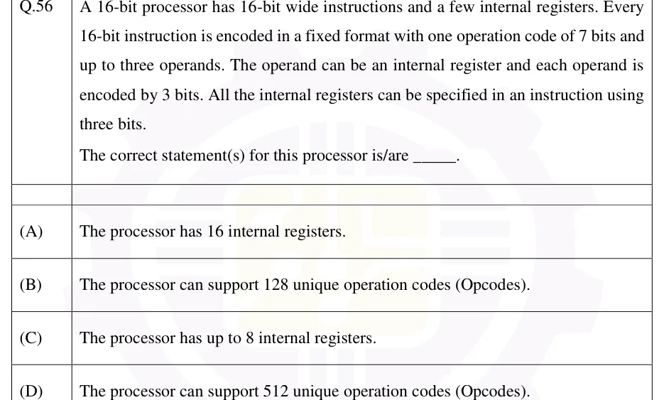
A 16-bit processor has 16-bit wide instructions and a few internal registers. Every 16-bit instruction is encoded in a fixed format with one operation code of 7 bits and up to three operands. The operand can be an internal register and each operand is encoded by 3 bits. All the internal registers can be specified in an instruction using three bits.
The correct statement(s) for this processor is/are ______.
The processor has 16 internal registers.
The processor can support 128 unique operation codes (Opcodes).
The processor has up to 8 internal registers.
The processor can support 512 unique operation codes (Opcodes).
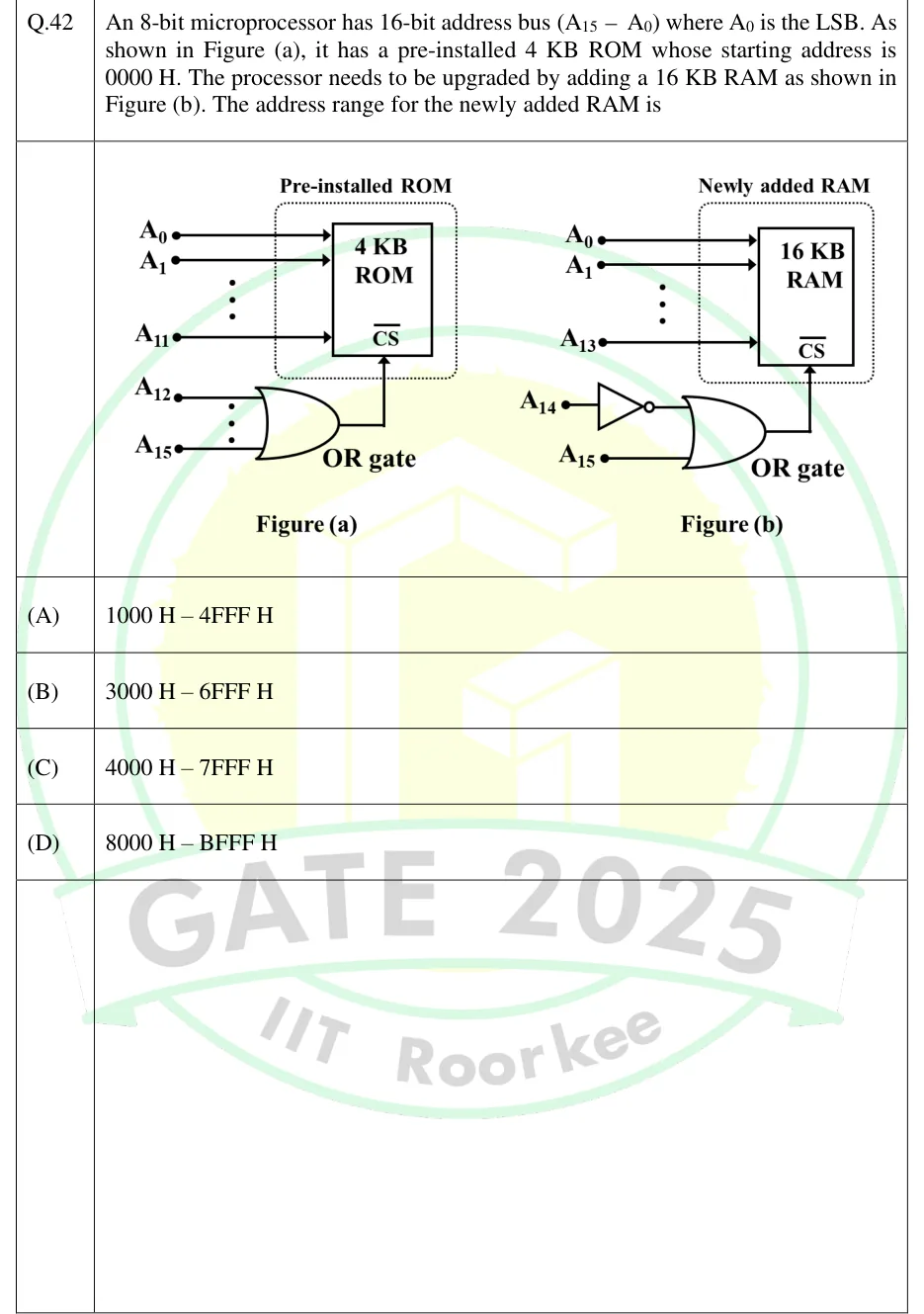
An 8-bit microprocessor has 16-bit address bus () where is the LSB. As shown in Figure (a), it has a pre-installed 4 KB ROM whose starting address is 0000 H. The processor needs to be upgraded by adding a 16 KB RAM as shown in Figure (b). The address range for the newly added RAM is
 Tap to open full size
Figure (a), labelled 'Pre-installed ROM': a block marked '4 KB ROM' inside a dotted box. Address lines A_0, A_1,, A_11 (vertical dots between A_1 and A_11) go straight into the ROM's address inputs. Lines A_12,, A_15 (vertical dots between) are the inputs of an OR gate. The OR gate output drives the ROM's active-low chip select CS. Figure (b), labelled 'Newly added RAM': a block marked '16 KB RAM' inside a dotted box. Address lines A_0, A_1,, A_13 (vertical dots between A_1 and A_13) go straight into the RAM's address inputs. A_14 passes through a NOT gate (inverter) into one input of a 2-input OR gate; A_15 goes directly into the other input. The OR gate output drives the RAM's active-low chip select CS.
1000 H – 4FFF H
3000 H – 6FFF H
4000 H – 7FFF H
8000 H – BFFF H
A machine has a 32-bit architecture with 1-word long instructions. It has 24 registers and supports an instruction set of size 40. Each instruction has five distinct fields, namely opcode, two source register identifiers, one destination register identifier, and an immediate value. Assuming that the immediate operand is an unsigned integer, its maximum value is ________.
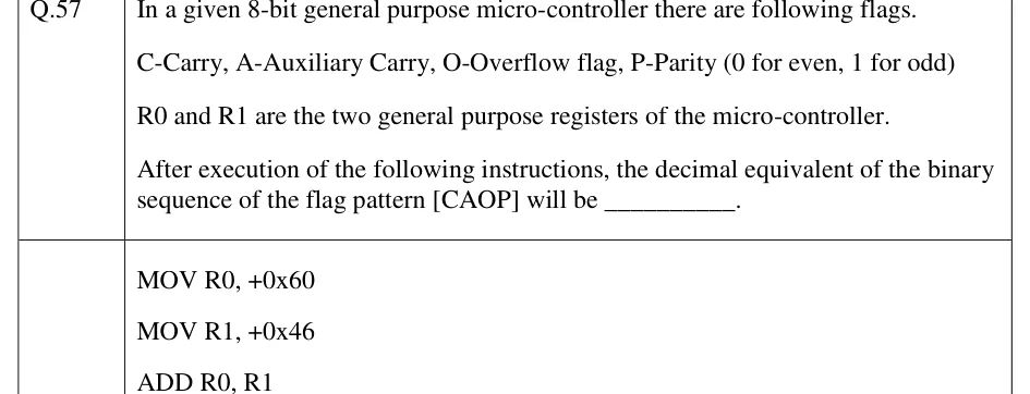
In a given 8-bit general purpose micro-controller there are following flags.
C-Carry, A-Auxiliary Carry, O-Overflow flag, P-Parity (0 for even, 1 for odd)
R0 and R1 are the two general purpose registers of the micro-controller.
After execution of the following instructions, the decimal equivalent of the binary sequence of the flag pattern [CAOP] will be ________.
MOV R0, +0x60
MOV R1, +0x46
ADD R0, R1
In an 8085 microprocessor, the number of address lines required to access a 16 K byte memory bank is ______.
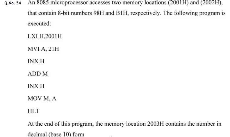
An 8085 microprocessor accesses two memory locations (2001H) and (2002H), that contain 8-bit numbers 98H and B1H, respectively. The following program is executed:
LXI H,2001H
MVI A, 21H
INX H
ADD M
INX H
MOV M, A
HLT
At the end of this program, the memory location 2003H contains the number in decimal (base 10) form ________.
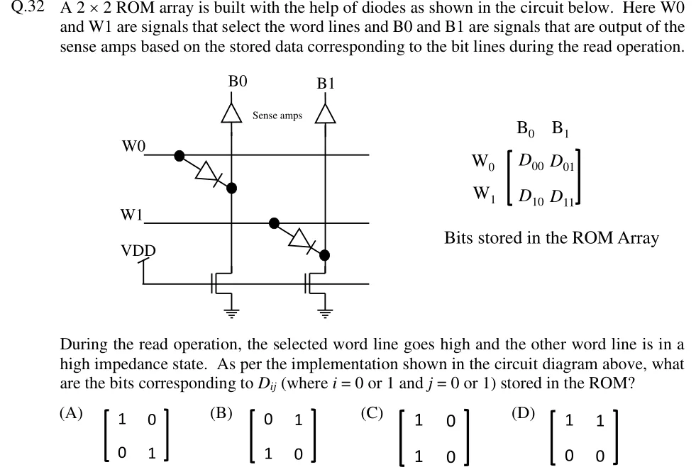
A ROM array is built with the help of diodes as shown in the circuit below. Here W0 and W1 are signals that select the word lines and B0 and B1 are signals that are output of the sense amps based on the stored data corresponding to the bit lines during the read operation.
[Figure: diode ROM array; beside it the matrix of bits stored in the ROM array, rows , columns : ]
During the read operation, the selected word line goes high and the other word line is in a high impedance state. As per the implementation shown in the circuit diagram above, what are the bits corresponding to (where or and or ) stored in the ROM?
 Tap to open full size
Two horizontal word lines, W0 (top) and W1 (below it), cross two vertical bit lines, B0 (left) and B1 (right). At the top of each bit line is an upward-pointing buffer triangle (labelled 'Sense amps') whose output is labelled B0 and B1. Diode 1: its anode connects to W0 at a dot to the left of B0, and its cathode connects to the B0 bit line at a dot just below W0. The diode symbol points from W0 toward B0. Diode 2: its anode connects to W1 at a dot between B0 and B1, and its cathode connects to the B1 bit line just below W1. There is no diode between W0 and B1, and none between W1 and B0. At the bottom of each bit line is an n-channel MOSFET. Its drain is on the bit line and its source goes to ground. A horizontal line labelled VDD drives the gates of both MOSFETs, so both are always on and act as pull-down loads on the bit lines. To the right is the matrix 'Bits stored in the ROM Array': row W0 = [D00 D01], row W1 = [D10 D11], columns B0 and B1.
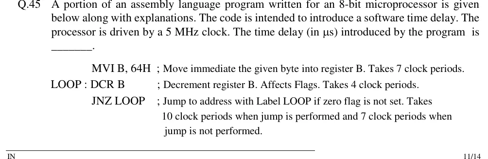
A portion of an assembly language program written for an 8-bit microprocessor is given below along with explanations. The code is intended to introduce a software time delay. The processor is driven by a 5 MHz clock. The time delay (in s) introduced by the program is ________.
        MVI B, 64H   ; Move immediate the given byte into register B. Takes 7 clock periods.
LOOP :  DCR B        ; Decrement register B. Affects Flags. Takes 4 clock periods.
        JNZ LOOP     ; Jump to address with Label LOOP if zero flag is not set. Takes
                     ; 10 clock periods when jump is performed and 7 clock periods when
; jump is not performed.PRACTICE
A non-pipelined processor has a total logic delay of 900 ps per instruction and completes one instruction every 900 ps. It is converted into a 5-stage pipeline with stage delays 150, 200, 180, 170 and 200 ps, and each pipeline latch adds 20 ps. In the program, 20% of the instructions are conditional branches, every branch causes 2 stall cycles, and there are no other stalls. For a very long program, the speed-up of the pipelined processor over the non-pipelined one is ______ (rounded to two decimal places).
Answer: (accepted range )
Clock period: ps.
.
Average time per instruction ps.
.
A word-addressable machine has register R1 = 200 and memory contents M[200] = 600, M[300] = 500, M[500] = 800, M[600] = 100, M[800] = 450 (all decimal). An instruction that loads register R2 has an address field containing 300; the addressing mode is as stated in each option, and indexed addressing adds R1 to the address field with no scaling. Which of the following statements is/are correct?
With direct addressing, R2 receives 500.
With memory-indirect addressing through the address field, R2 receives 800.
With register-indirect addressing through R1, R2 receives 100.
With indexed addressing (address field + R1), R2 receives 800.
Answer: (A), (B), (D)
Direct: EA = 300, operand M[300] = 500. A is correct.
Memory indirect: EA = M[300] = 500, operand M[500] = 800. B is correct.
Register indirect: EA = R1 = 200, operand M[200] = 600, not 100 (reaching M[600] would need a second level of indirection). C is wrong.
Indexed: EA = 300 + 200 = 500, operand M[500] = 800. D is correct.
Which one of the following statements about semiconductor memories is correct?
A DRAM cell stores its bit as charge on a capacitor; reading disturbs that charge, so the sensed value is written back.
A 6T SRAM cell must be refreshed periodically because charge leaks from its cross-coupled inverters.
An EPROM is erased electrically, one byte at a time, without removing it from the circuit.
For the same chip area, an SRAM stores more bits than a DRAM because its cell needs no capacitor.
Answer: (A)
A is correct: the 1T1C read is destructive, and the sense amplifier restores the value.
B is wrong: the latch actively holds its state, so SRAM needs no refresh.
C is wrong: that describes EEPROM; an EPROM is erased by ultraviolet light, whole chip at once.
D is wrong: the 6-transistor cell is much larger than the 1T1C cell, so DRAM is denser.
In an 8085 system, a memory chip has its address pins connected to , and its is asserted only when , , and (full decoding). The address range occupied by the chip is
A000H to AFFFH
B000H to BFFFH
B000H to B7FFH
D000H to DFFFH
Answer: (B)
Select pattern = BH, read MSB first.
All chip lines 0 gives B000H; all chip lines 1 gives BFFFH.
Check: BFFFH − B000H + 1 = 1000H = 4096 = 4K. Option D reads the select bits in reverse order; option C is the size of a 2K chip.
An 8085 microprocessor is driven by a 6 MHz crystal. It executes the following code once: MVI C, 64H (7 T-states); LOOP: DCR C (4 T-states); JNZ LOOP (10 T-states if the jump is taken, 7 T-states if it is not). The total execution time of this code, in microseconds, is ______.
Answer: (accepted range )
64H = 100, so the loop body runs N = 100 times and JNZ is taken 99 times.
T-states .
Clock MHz, so one T-state lasts .
Time .
OFFICIAL GATE 2027 SYLLABUS WORDING
Copied from the GATE 2027 syllabus; see all 2027 syllabi.
GATE EC
Semiconductor Memories: ROM, SRAM, DRAM. Computer Organization: Machine instructions and addressing modes, ALU, data-path and control unit, instruction pipelining
GATE IN
embedded systems: common microprocessors and microcontrollers, memory and input-output interfacing, embedded systems programming; basics of data acquisition systems, virtual instrumentation, IoT
Preparing in Kolkata? IAE Academy's course for GATE ECE or GATE IN.