
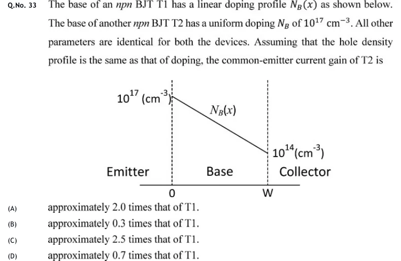
The base of an npn BJT T1 has a linear doping profile as shown below. The base of another npn BJT T2 has a uniform doping of . All other parameters are identical for both the devices. Assuming that the hole density profile is the same as that of doping, the common-emitter current gain of T2 is
 Tap to open full size
Figure description
Doping profile of the base of T1. Two vertical dashed lines mark x = 0 (the Emitter/Base boundary) and x = W (the Base/Collector boundary) on a horizontal axis marked 0 and W, with the regions labelled Emitter, Base and Collector. A straight line labelled N_B(x) falls linearly from 10^17 (cm^-3) at x = 0 to 10^14 (cm^-3) at x = W. There is no labelled vertical axis; only these two values are marked.
- (A)
approximately 2.0 times that of T1.
- (B)
approximately 0.3 times that of T1.
- (C)
approximately 2.5 times that of T1.
- (D)
approximately 0.7 times that of T1.