IAE Academy

GATE EC

The bipolar junction transistor as a device

A bipolar junction transistor (BJT) has three terminals: emitter, base and collector. It amplifies because a heavily doped emitter injects carriers into a thin base, and most of them survive to reach the collector. This topic covers the quantities that describe how efficiently that happens: emitter injection efficiency, base transport factor, α and β, and the leakage currents and . It also covers the Ebers–Moll model, with its sign conventions, which describes the device in every mode of operation. Finally, it covers the non-idealities that make a real device depart from an ideal current source: base-width modulation, the Early effect, punch-through and collector breakdown. The same quantities underlie biasing, small-signal models and amplifier stages, so getting the conventions and the operating-region conditions right here carries through to every later BJT topic.

3 previous-year questions · 2 solved · 6 practice questions

BJT Structure, Doping and Modes of Operation

A bipolar junction transistor (BJT) has three regions and two pn junctions. The middle region, the base, is shared by both junctions and is thin. For an npn device the layers are n (emitter), p (base), n (collector); for a pnp device they are p, n, p. The terminals are the emitter (E), base (B) and collector (C). The two junctions are the emitter-base junction (EBJ) and the collector-base junction (CBJ). Two separate diodes wired back to back do not behave as a transistor. Transistor action needs the base to be much thinner than the minority-carrier diffusion length, so that carriers injected at the EBJ can diffuse across it to the CBJ before they recombine.

Doping pattern of a typical BJT (npn shown)

  1. Emitter: heavily doped (written for an npn). Making is what brings the emitter injection efficiency close to 1.

  2. Base: doped more lightly than the emitter, and physically thin (, the minority-carrier diffusion length in the base). The thin base is what brings the base transport factor close to 1.

  3. Collector: in a device designed for a high collector-base breakdown voltage, the collector next to the CBJ is the most lightly doped region (). The CBJ depletion region then lies mainly in the collector. That raises the breakdown voltage, reduces base-width modulation (the Early effect) and delays punch-through. A heavily doped region further from the junction (the sub-collector) keeps the collector's series resistance low.

  4. Some introductory treatments rank the collector doping between the emitter and the base. The physical requirement that the CBJ depletion region extend mainly into the collector is what the lighter collector doping achieves.

Modes of operation of an npn BJT (forward bias positive; for a pnp every voltage and current reverses)

Mode

EBJ bias

CBJ bias

Behaviour

Active (forward-active)

Forward

Reverse

; the region used for amplification

Saturation

Forward

Forward

Switch 'on' state; small; (the forced is below )

Cut-off

Reverse

Reverse

Switch 'off' state; only leakage currents flow

Reverse-active

Reverse

Forward

Roles of E and C interchanged; because the device is not symmetric

Current Components in Active Mode

Take an npn device in active mode. The forward-biased EBJ injects electrons from the emitter, where they are majority carriers, into the base, where they are minority carriers. Call this electron current . At the same time the base injects holes back into the emitter, giving a current . This current does not reach the collector. Of the electrons injected into the base, a fraction recombines in the base, and the remainder, , reaches the CBJ and is swept into the collector. The base current supplies both losses: the back-injected holes and the holes lost to recombination. With recombination in the EBJ depletion region neglected, , where is the reverse leakage of the CBJ. Two figures of merit describe these losses.

EMITTER INJECTION EFFICIENCY

This is the fraction of the emitter current made up of carriers injected into the base. It assumes recombination in the EBJ depletion region is negligible. It is made close to 1 by doping the emitter much more heavily than the base.

INJECTION EFFICIENCY IN TERMS OF DESIGN PARAMETERS (NPN)

Here is the hole diffusion coefficient in the emitter, the electron diffusion coefficient in the base, and , the neutral emitter and base widths. The expression assumes uniform doping, low-level injection and short regions (, ). For a long emitter, replace by .

BASE TRANSPORT FACTOR

This is the fraction of carriers injected into the base that survive recombination and reach the CBJ. The sech form assumes uniform base doping and low-level injection. The approximation holds for , where and is the minority-carrier lifetime in the base.

COMMON-BASE CURRENT GAIN

This applies in active mode with no avalanche multiplication at the CBJ (multiplication factor ). When is negligible, . For a real device , and it is close to 1.

COMMON-EMITTER CURRENT GAIN

When is negligible, . The second form holds when and are both close to 1, and it shows how the two losses add. Because is close to 1, is very sensitive to small changes in . Carry enough significant figures in before dividing.

TERMINAL CURRENT RELATIONS (ACTIVE MODE, LEAKAGE NEGLECTED)

The first relation is KCL for the whole device (currents taken into C and B and out of E for an npn). The others convert between and and give any one of , , from another. A useful identity is .

LEAKAGE CURRENTS

is the collector current with the emitter open and the CBJ reverse-biased. is the collector current with the base open. is larger by a factor of because the leakage current, flowing into the base, is itself amplified. Both relations hold in active mode.

Ebers–Moll Model

The Ebers–Moll model treats a BJT as two coupled diodes, the EBJ and the CBJ. It applies in all modes: active, saturation, cut-off and reverse-active. The active-mode formulas of the previous section are a special case of it. Conventions used here (npn): flows into the collector terminal, flows into the base, and flows out of the emitter, so that . Junction voltages and are measured p-side minus n-side, so forward bias is positive. at 300 K.

EBERS–MOLL EMITTER CURRENT (NPN)

is the EBJ saturation current measured with the collector shorted to the base. is the reverse (inverse) common-base current gain.

EBERS–MOLL COLLECTOR CURRENT (NPN)

is the forward common-base gain, the used elsewhere in this topic. is the CBJ saturation current measured with the emitter shorted to the base.

RECIPROCITY CONDITION

This follows from the reciprocity of the device. It reduces the four Ebers–Moll parameters to three independent ones, and it defines the transport saturation current .

ACTIVE-MODE REDUCTION

These hold when the EBJ is forward-biased with several times , so the is negligible, and , so the CBJ diode term contributes at most a small leakage. They follow from the Ebers–Moll equations using and . This is the exponential law used for the active-mode – characteristic.

SATURATION CURRENT IN TERMS OF DEVICE PARAMETERS (NPN)

is the emitter area, the electron diffusion coefficient in the base, the uniform base doping, the neutral base width and the intrinsic concentration (about for Si at 300 K). It assumes a short base (), so the minority-carrier profile in the base is linear, and low-level injection. Because , narrowing the neutral base raises . That is the Early effect.

BASE TRANSIT TIME AND ITS LINK TO Β

is the average time a minority carrier takes to diffuse across a short base. is the minority-carrier lifetime in the base. The expression for holds when base recombination is the only significant loss (): then .

EXAM TIP

Two rules of thumb for silicon at room temperature. At constant , falls by roughly 2 mV for each 1 °C rise in temperature. roughly doubles for every 10 °C rise. Use them only for estimates.

Early Effect and Output Resistance

The active-mode formulas above make independent of , which treats the BJT as an ideal current source. In a real device, rises slightly with at fixed . This is the Early effect. It is caused by base-width modulation (next section), and it gives a BJT a finite output resistance.

EARLY EFFECT: COLLECTOR CURRENT

This first-order model holds in active mode at constant . is the current extrapolated to . is the Early voltage. Extending the straight-line – characteristic back to the axis gives a crossing at .

SMALL-SIGNAL OUTPUT RESISTANCE

It is evaluated at the DC operating point, in active mode. The middle expression follows exactly from the model above. The approximation is the one normally used, and it holds when .

EXAM TIP

In this first-order model is a property of the transistor and does not depend on the bias point. At different bias points of the same transistor, therefore scales inversely with .

Base-Width Modulation, Punch-Through and Breakdown

The physical cause of the Early effect is base-width modulation. In active mode the CBJ is reverse-biased, with reverse bias . Its depletion region extends into each side in inverse proportion to that side's doping: mostly into the lightly doped collector, but partly into the base. When is raised at fixed , rises, the depletion region extends further into the base, and the neutral (quasi-neutral) base width shrinks.

NEUTRAL BASE WIDTH VS BIAS

is the metallurgical base width, measured junction to junction. and are the parts of the EBJ and CBJ depletion widths that lie in the base. For a step junction, grows as , where is the CBJ built-in potential and is reverse bias. With fixed, does not change.

For a short base, . A smaller neutral base width therefore gives a steeper minority-carrier gradient and a larger , which is exactly the Early effect. Punch-through is the extreme limit of the same mechanism. If the reverse bias is raised far enough, the CBJ depletion region takes up the entire neutral base and merges with the EBJ depletion region. The barrier that controls injection from the emitter is then lost, and the collector current rises sharply. This is a breakdown-like effect caused by depletion reach-through, not by avalanche multiplication. A base doped more heavily than the collector keeps small, which delays punch-through.

COLLECTOR-EMITTER BREAKDOWN WITH THE BASE OPEN

is the avalanche breakdown voltage of the CBJ with the emitter open. is an empirical constant, typically between 3 and 6. With the base open, the avalanche current is amplified by the transistor's gain, so breakdown occurs at a lower voltage than for the isolated junction: .

EXAM TIP

Exam trap: punch-through and avalanche breakdown (, ) both show a sharp rise in current at high collector voltage, but their causes differ. Punch-through is set by the base width and the base and collector doping: the depletion regions merge. Avalanche breakdown is carrier multiplication in the high field at the CBJ. Do not treat them as the same effect.

Worked Examples

WORKED EXAMPLE

A silicon npn BJT in active mode has and . Neglecting , find , and .

Solution
  1. . Check: , which agrees.

Answer: , , .

WORKED EXAMPLE

A BJT in active mode has Early voltage . With fixed and , the measured current is . Estimate at the same when .

Solution
  1. Use . is the same, so is the same, and it cancels in the ratio:

  2. Cross-check with the output resistance: , so . This agrees.

Answer: . That is about a 6% rise in for a 5 V increase in , which shows why is large but finite.

WORKED EXAMPLE

An npn BJT in active mode has a neutral base width equal to one-tenth of the electron diffusion length in the base () and an emitter injection efficiency . Estimate , and , neglecting leakage.

Solution
  1. . The exact value agrees.

  2. Check with , giving . This is close; the small gap arises because the check is only a first-order approximation.

Answer: , , . Here the injection efficiency, not base recombination, is the larger loss.

PREVIOUS-YEAR QUESTIONS

3 questions from the EC papers

Try each question first, then open the answer. One shows the official answer only. We placed each question under a topic ourselves; the exam paper does not label topics.

See these papers in full: GATE ECE 2026 · GATE ECE 2024 · GATE ECE 2020

GATE 2026 EC Q.29

GATE 2026 · ECQ.29 · 1 mark · MSQ

Figure shows the output characteristics of two different Bipolar Junction Transistors (BJT), BJT 1 with magnitude of Early voltage , and BJT 2 with magnitude of Early voltage .

Which of the following options is/are correct regarding the Early voltages?
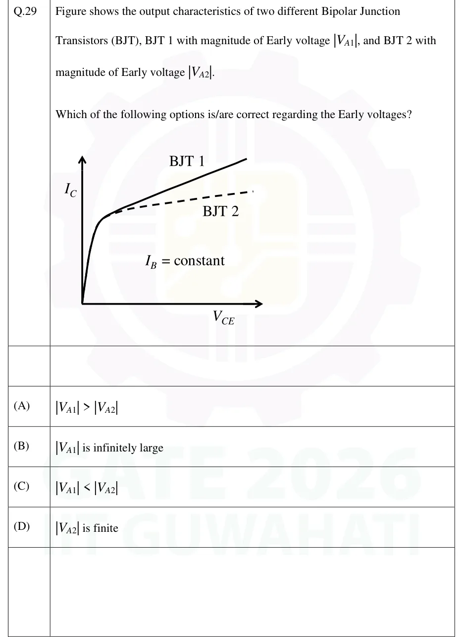
GATE 2026 EC question 29: A plot of collector current I_C (vertical axis) versus collector-emitter voltage V_CE (horizontal axis), both axes…Tap to open full size
Figure from the GATE 2026 EC paper. It is part of the question.
Figure description

A plot of collector current I_C (vertical axis) versus collector-emitter voltage V_CE (horizontal axis), both axes unlabeled with numeric values (arrows only, origin at bottom-left). Both curves are drawn for a constant base current, I_B = constant (labeled inside the plot). Both curves start at the origin, rise steeply through a curved knee region (the saturation-to-active transition), and then continue upward in the active region as straight, gently-rising lines. The curve labeled 'BJT 1' (solid line) has the steeper slope in the active region and ends higher/further right at the top of the plot. The curve labeled 'BJT 2' (dashed line) branches off from the same knee point as BJT 1 but has a distinctly flatter (much smaller) slope in the active region, ending lower and shorter than BJT 1's curve.

  1. (A)

  2. (B)

    is infinitely large

  3. (C)

  4. (D)

    is finite

Answer and solution
GATE 2026 EC Q.29: answer and solution

GATE 2024 EC Q.52

GATE 2024 · ECQ.52 · 2 marks · MSQ

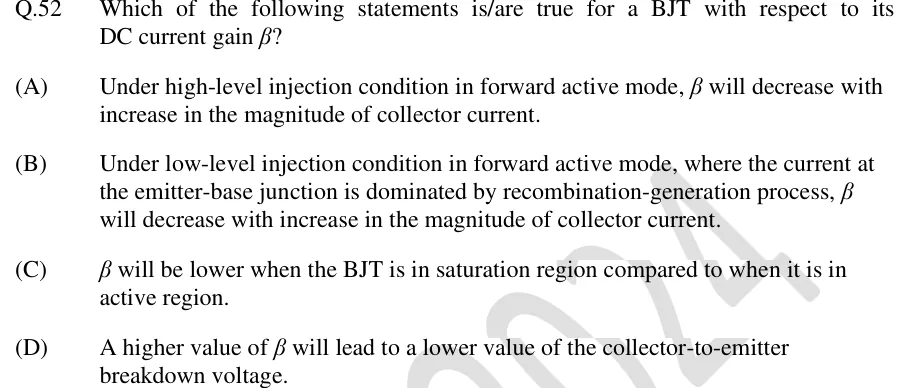
Which of the following statements is/are true for a BJT with respect to its DC current gain ?

  1. (A)

    Under high-level injection condition in forward active mode, will decrease with increase in the magnitude of collector current.

  2. (B)

    Under low-level injection condition in forward active mode, where the current at the emitter-base junction is dominated by recombination-generation process, will decrease with increase in the magnitude of collector current.

  3. (C)

    will be lower when the BJT is in saturation region compared to when it is in active region.

  4. (D)

    A higher value of will lead to a lower value of the collector-to-emitter breakdown voltage.

Answer and solution
See the question in the paper
GATE 2024 EC Q.52: answer and solution

GATE 2020 EC Q.33

GATE 2020 · ECQ.33 · 2 marks · MCQ

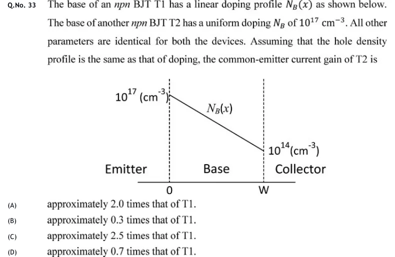
The base of an npn BJT T1 has a linear doping profile as shown below. The base of another npn BJT T2 has a uniform doping of . All other parameters are identical for both the devices. Assuming that the hole density profile is the same as that of doping, the common-emitter current gain of T2 is

GATE 2020 EC question 33: Doping profile of the base of T1.Tap to open full size
Figure from the GATE 2020 EC paper. It is part of the question.
Figure description

Doping profile of the base of T1. Two vertical dashed lines mark x = 0 (the Emitter/Base boundary) and x = W (the Base/Collector boundary) on a horizontal axis marked 0 and W, with the regions labelled Emitter, Base and Collector. A straight line labelled N_B(x) falls linearly from 10^17 (cm^-3) at x = 0 to 10^14 (cm^-3) at x = W. There is no labelled vertical axis; only these two values are marked.

  1. (A)

    approximately 2.0 times that of T1.

  2. (B)

    approximately 0.3 times that of T1.

  3. (C)

    approximately 2.5 times that of T1.

  4. (D)

    approximately 0.7 times that of T1.

Official answer

Official answer: marks to all candidatesSource: Official answer key, GATE 2020 EC (IIT Delhi)

GATE 2020 EC Q.33: official answer

PRACTICE

6 questions to test yourself

PRACTICE 11 mark · MCQ

A silicon BJT operating in active mode has emitter injection efficiency and base transport factor . Neglecting and avalanche multiplication, the common-emitter current gain is closest to:

  1. (A)

    71

  2. (B)

    100

  3. (C)

    142

  4. (D)

    200

Answer and solution

Answer: (C)

  1. , so the answer is (C).

  2. This shows why a small change in near 1 causes a large change in .

PRACTICE 21 mark · NAT

A BJT operating in active mode has emitter current and common-base current gain . Neglecting , find the base current in mA.

Answer and solution

Answer: (accepted range )

  1. KCL for the device:

PRACTICE 32 marks · MSQ

For an npn BJT biased in active mode, which of the following statements about the Early effect are correct?

  1. (A)

    Increasing decreases the effective neutral base width

  2. (B)

    Increasing increases for a fixed

  3. (C)

    The Early effect is modelled by a finite output resistance, approximately

  4. (D)

    The Early effect arises from modulation of the emitter-base depletion width by

Answer and solution

Answer: (A), (B), (C)

  1. Increasing with fixed increases the CBJ reverse bias . The CBJ depletion region widens into the base, and the neutral base width shrinks. (A is correct.)

  2. A narrower neutral base steepens the minority-carrier gradient in the base, so increases for the same . (B is correct.)

  3. The finite slope of against is modelled by an output resistance in the small-signal model. (C is correct.)

  4. The Early effect comes from modulation of the collector-base depletion width. The emitter-base depletion width is set by , which is held fixed, so D is false.

PRACTICE 41 mark · NAT

A BJT in active mode has Early voltage . At an operating point with , the collector current is . Using the standard approximation , find the small-signal output resistance in .

Answer and solution

Answer: (accepted range )

  1. The model gives exactly . The approximation drops because .

PRACTICE 51 mark · MCQ

Punch-through in an npn BJT occurs when:

  1. (A)

    The emitter-base depletion region reaches the collector

  2. (B)

    The collector-base depletion region extends completely across the neutral base and reaches the emitter-base depletion region

  3. (C)

    Avalanche multiplication occurs at the collector-base junction

  4. (D)

    The base transport factor becomes negative

Answer and solution

Answer: (B)

  1. Increasing the collector-base reverse bias widens the CBJ depletion region into the thin base.

  2. If the reverse bias is large enough, this depletion region extends across the whole neutral base and meets the EBJ depletion region. That is punch-through, so the answer is (B).

  3. It is a depletion reach-through effect, distinct from avalanche multiplication, which is carrier multiplication in the high field at the junction. is a fraction between 0 and 1 and cannot become negative.

PRACTICE 61 mark · NAT

An npn BJT has and collector-base leakage current . With the base terminal open and the transistor in active mode, find the collector-emitter leakage current in nA.

Answer and solution

Answer: (accepted range )

  1. With the base open, , so .

OFFICIAL GATE 2027 SYLLABUS WORDING

Copied from the GATE 2027 syllabus; see all 2027 syllabi.

GATE EC

BJT

Preparing in Kolkata? IAE Academy's course for GATE ECE.