IAE Academy

GATE EC

LEDs, photodiodes and solar cells

This topic covers how a p-n junction converts between light and electrical energy. An LED turns forward-bias current into light and needs a direct band gap. A photodiode turns incident light into a photocurrent, usually under reverse bias, and is described by its quantum efficiency and responsivity. A solar cell turns light into electrical power delivered to a load, and is described by its I-V curve, open-circuit voltage, short-circuit current, fill factor and efficiency. All three rest on the photon energy compared with the band gap , so keep energies in eV, use , and fix the current sign convention before solving.

5 previous-year questions · 5 solved · 6 practice questions

Optical Absorption and the Band Gap

A photon incident on a semiconductor can be absorbed across the band gap, creating an electron-hole pair, only if its energy is at least the band gap . This single condition links all three devices in this topic: an LED uses the reverse process (an electron and hole recombine and emit a photon), while photodiodes and solar cells use absorption to generate carriers. The photon energy and the band gap of the material therefore fix the wavelength range each device works over.

Conventions used throughout this topic: energies in eV; electron charge C; ; thermal voltage mV at 300 K; applied voltage is positive for forward bias (p side positive).

PHOTON ENERGY

Holds for a photon of free-space wavelength . Numeric form: .

PHOTON FLUX

Number of photons per second carried by monochromatic light of optical power (W). With in eV, .

CUTOFF WAVELENGTH

Band-to-band absorption occurs only for (i.e. ). For there is no band-to-band absorption; the material is nearly transparent apart from weaker impurity and free-carrier absorption.

ABSORPTION WITH DEPTH

is the absorption coefficient (cm), which depends on wavelength; is the penetration depth. The fraction of the light entering the material that is absorbed within a thickness is .

EXAM TIP

Keep in eV and use directly. Plug in J·s only when the energy is needed in joules, and then convert with J.

Light Emitting Diodes (LEDs)

An LED is a forward-biased p-n junction. Forward bias injects electrons into the p side and holes into the n side; these injected minority carriers recombine within about a diffusion length of the junction (or inside a thin active layer in a heterostructure LED), and radiative recombination emits a photon of energy close to . Efficient LED action requires a direct band gap material: the conduction-band minimum and the valence-band maximum occur at the same crystal momentum, so an electron and a hole can recombine by emitting only a photon. In an indirect-gap material (Si, Ge, GaP) band-to-band recombination also needs a phonon to conserve momentum, so radiative recombination is far less probable than non-radiative recombination through traps; these materials make poor LEDs unless special impurities are added (for example nitrogen in GaP).

LED EMISSION (PEAK) WAVELENGTH

For band-to-band emission in a direct-gap material. The emitted photon energy is close to, and slightly above, because the injected carriers are spread over a few above the band edges; this also gives the emission a finite spectral width.

INTERNAL QUANTUM EFFICIENCY

Fraction of recombination events that emit a photon. , are the radiative and non-radiative recombination rates; , the corresponding lifetimes, with total lifetime .

LED OPTICAL OUTPUT POWER

is the forward current and the photon energy (J). (external quantum efficiency) is photons leaving the device per electron passing through it; is the fraction of the current that recombines in the active region, and the fraction of generated photons that escape. With in eV: (W, with in A).

CRITICAL ANGLE AT THE SEMICONDUCTOR-AIR SURFACE

Light striking the top surface at more than from the normal is totally internally reflected. For a typical III-V semiconductor (), , which is why only a small fraction of the generated light escapes a planar LED. At normal incidence the reflected fraction is .

Points to remember about LED operation

  1. The junction must be forward biased so that minority carriers are injected across it and recombine near it.

  2. A direct band gap is needed for high internal quantum efficiency.

  3. The emission wavelength is set, to first order, by of the light-emitting (active) region, not by the operating current. It shifts slightly with temperature because falls as temperature rises.

  4. The forward voltage at which an LED conducts appreciably is roughly : a wider-gap (shorter-wavelength) LED needs a higher forward voltage.

  5. External quantum efficiency is lower than internal quantum efficiency because of re-absorption inside the chip, Fresnel reflection at the surface and total internal reflection beyond the critical angle.

  6. Alloying tunes , and hence colour, within a material family, but the gap can change from direct to indirect with composition: is direct only up to about ( eV).

Approximate room-temperature band gaps and emission (illustrative values)

Material

Approx. (eV)

Nature

Approx.

Region

Si

1.12

Indirect

≈1.11 μm

Not used for LEDs (indirect)

GaAs

1.42

Direct

≈0.87 μm

Near-infrared

≈1.9

Direct

≈0.65 μm

Red

GaP

2.26

Indirect

≈0.55 μm

Weak emission unless N-doped (green/yellow-green)

InGaN (In fraction set so eV)

≈2.7

Direct

≈0.46 μm

Blue

GaN

3.4

Direct

≈0.365 μm

Near-ultraviolet

WORKED EXAMPLE

A GaAs LED has eV. Estimate its peak emission wavelength and state whether it is visible.

Solution
  1. The visible range is roughly 400 nm to 700 nm, so 873 nm lies in the near-infrared.

Answer: ≈ 873 nm, near-infrared (not visible)

WORKED EXAMPLE

An LED emitting at nm has external quantum efficiency and carries a forward current of 20 mA. Find the optical output power.

Solution
  1. Photon energy: eV

  2. Electrons per second:

  3. W

Answer: mW

Photodiodes

A photodiode is a p-n (or p-i-n) junction in which absorbed photons generate electron-hole pairs; pairs generated in or near the depletion region are separated by its field and give a photocurrent. It is usually operated under reverse bias (photoconductive mode), where the output current is proportional to the incident optical power and the response is fast. It can also be operated with no external bias (photovoltaic mode), where the light itself develops a voltage across the junction; a solar cell works this way.

ILLUMINATED P-N JUNCTION (CURRENT INTO THE P TERMINAL POSITIVE)

is positive for forward bias; is the current flowing into the p terminal from the external circuit (the usual diode convention). is the reverse saturation (dark) current, the ideality factor ( ideal) and mV at 300 K. The photocurrent flows in the reverse direction and simply adds to the dark characteristic, which shifts the whole I-V curve down by . Assumes does not depend on and neglects series and shunt resistance.

PHOTOCURRENT

is the incident optical power (W) and the quantum efficiency. Assumes no internal gain (each collected pair gives one electron of external current), i.e. not an avalanche photodiode.

QUANTUM EFFICIENCY

Electron-hole pairs collected per second divided by photons incident per second; without internal gain. It is reduced by surface reflection, by light passing through without being absorbed, and by carriers recombining before they are collected. Ignoring collection losses, , where is the surface reflectance and the absorbing (depletion) width.

RESPONSIVITY

Holds for ; beyond the cutoff wavelength , and so , falls to nearly zero. At constant the responsivity rises linearly with (a longer-wavelength photon carries less energy, so a watt contains more photons), then drops sharply near . The maximum possible value, at , is A/W.

AVALANCHE PHOTODIODE (APD)

An APD is reverse biased close to breakdown so that impact ionisation multiplies each photogenerated carrier; is the average multiplication (gain) factor. Its responsivity can therefore exceed the limit of an ordinary photodiode.

Why reverse bias is used (photoconductive mode)

  1. Reverse bias ( with forward taken as positive) widens the depletion region; for an abrupt junction , where is the built-in potential (positive).

  2. With a wider, higher-field depletion region, more photons are absorbed where carriers are swept out by drift, instead of in the neutral regions where they must diffuse slowly to the junction. Removing this slow diffusion component is what speeds up the response.

  3. Junction capacitance falls as increases, raising the RC-limited bandwidth.

  4. A very wide depletion region lengthens the drift transit time (), so the width is a design trade-off; the p-i-n structure fixes a wide intrinsic layer for this reason.

  5. Under reverse bias with , ; since normally , , which is proportional to .

  6. Reverse bias does not remove the dark current. The dark current and its noise set the smallest optical power the photodiode can detect.

EXAM TIP

Do not confuse quantum efficiency (dimensionless, pairs per photon) with responsivity (A/W, current per unit optical power). A question may give one and ask for the other; convert with .

WORKED EXAMPLE

A Si photodiode ( eV) with quantum efficiency is illuminated at nm with optical power 2 mW. Find the responsivity and the photocurrent.

Solution
  1. Check the cutoff: , and , so the light is absorbed.

Answer: A/W, mA

Solar Cells

A solar cell is a p-n junction operated in photovoltaic mode, with no external source, delivering power to a load. Under illumination the junction's I-V curve is shifted down by the photocurrent into the fourth quadrant (positive , negative in the diode convention above), where : the device delivers power instead of absorbing it. For solar cells it is usual to count the current delivered to the load as positive, , which flips that part of the curve into the first quadrant. The cell's photocurrent is written (the same quantity as ).

SOLAR CELL EQUATION (CURRENT DELIVERED TO THE LOAD POSITIVE)

is the terminal voltage (positive, since the cell forward biases itself), is the current delivered to the external load, positive for . is the reverse saturation (dark) current, the ideality factor ( ideal) and mV at 300 K. Ideal model: series and shunt resistance neglected, independent of .

SHORT-CIRCUIT CURRENT

For a fixed spectrum, is proportional to the incident optical power (photon flux), so is too. The ideal model is assumed (no series resistance).

OPEN-CIRCUIT VOLTAGE

Obtained by setting . grows only logarithmically with light intensity: multiplying the intensity by raises by . falls as temperature rises, because (proportional to ) rises steeply with temperature.

MAXIMUM POWER POINT (IDEAL CELL)

From with . The maximum power point lies on the curve between and , with and .

FILL FACTOR

Ratio of the maximum-power rectangle to the rectangle . Always , since and . It is reduced by series resistance and by low shunt resistance.

CONVERSION EFFICIENCY

is the total optical power incident on the cell, under the same illumination at which and are measured.

Key solar-cell quantities (ideal model)

Quantity

Defined at

Depends primarily on

Incident optical power / photon flux ()

: logarithmic in light intensity; falls with rising temperature

Shape of the I-V curve between the two intercepts

How 'square' the I-V curve is; reduced by series resistance and low shunt resistance

WORKED EXAMPLE

A solar cell has mA and V; at its maximum power point V and mA. The incident optical power is 100 mW. Find the fill factor and the efficiency.

Solution

Answer: ,

WORKED EXAMPLE

An ideal solar cell () at 300 K has A and mA. Find (take mV).

Solution
  1. V

Answer: V

Summary and Exam Traps

LED vs photodiode vs solar cell

Device

Bias / operating point

Function

Key parameter

LED

Forward biased (first quadrant)

Electrical energy → light (injection + radiative recombination)

;

Photodiode

Reverse biased (photoconductive, third quadrant) or unbiased (photovoltaic)

Light → photocurrent (detector)

Responsivity

Solar cell

, delivering power to a load (fourth quadrant in the diode convention)

Light → electrical power (generator)

, , , efficiency

EXAM TIP

Fix the sign convention before solving a numerical. In the diode convention (current into the p terminal positive, forward bias positive) the photocurrent enters as : in a reverse-biased photodiode it adds to the reverse dark current, and in a solar cell it makes negative while is positive, so the cell delivers power. Solar-cell formulas are usually written with the delivered current taken as positive.

EXAM TIP

Only a direct band gap material gives an efficient band-to-band LED. For an indirect-gap material such as Si or Ge, radiative recombination is inefficient because momentum conservation needs a phonon, so non-radiative recombination dominates.

EXAM TIP

Check the wavelength against the cutoff before computing a photocurrent: light with gives essentially no band-to-band photocurrent, however high its power.

PREVIOUS-YEAR QUESTIONS

5 questions from the EC papers

Try each question first, then open the answer. We placed each question under a topic ourselves; the exam paper does not label topics.

See these papers in full: GATE ECE 2026 · GATE ECE 2024 · GATE ECE 2020 · GATE ECE 2018

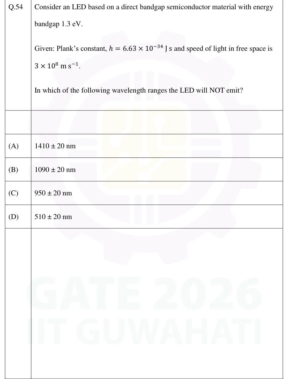
GATE 2026 EC Q.54

GATE 2026 · ECQ.54 · 2 marks · MSQ

Consider an LED based on a direct bandgap semiconductor material with energy bandgap 1.3 eV.

Given: Plank's constant, J s and speed of light in free space is .

In which of the following wavelength ranges the LED will NOT emit?

  1. (A)

    nm

  2. (B)

    nm

  3. (C)

    nm

  4. (D)

    nm

Answer and solution
See the question in the paper
GATE 2026 EC Q.54: answer and solution

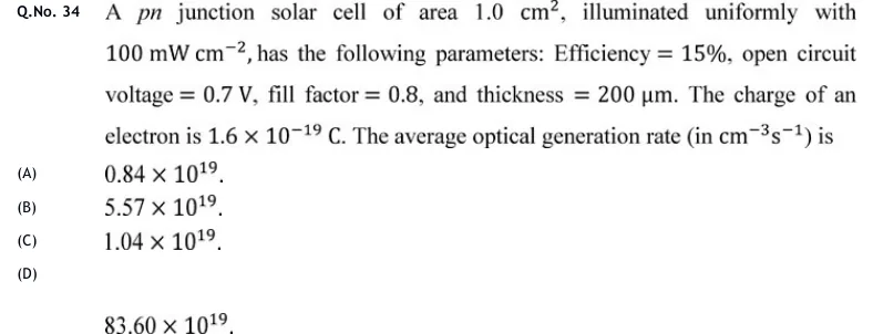
GATE 2020 EC Q.34

GATE 2020 · ECQ.34 · 2 marks · MCQ

A junction solar cell of area , illuminated uniformly with , has the following parameters: Efficiency , open circuit voltage , fill factor , and thickness . The charge of an electron is . The average optical generation rate (in ) is

  1. (A)

  2. (B)

  3. (C)

  4. (D)

Answer and solution
See the question in the paper
GATE 2020 EC Q.34: answer and solution

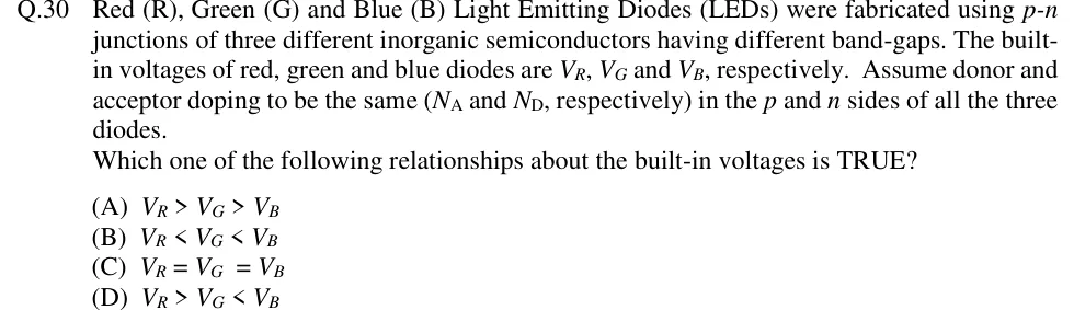
GATE 2018 EC Q.30

GATE 2018 · ECQ.30 · 2 marks · MCQ

Q.30 Red (R), Green (G) and Blue (B) Light Emitting Diodes (LEDs) were fabricated using - junctions of three different inorganic semiconductors having different band-gaps. The built-in voltages of red, green and blue diodes are , and , respectively. Assume donor and acceptor doping to be the same ( and , respectively) in the and sides of all the three diodes.

Which one of the following relationships about the built-in voltages is TRUE?

  1. (A)

  2. (B)

  3. (C)

  4. (D)

Answer and solution
See the question in the paper
GATE 2018 EC Q.30: answer and solution

GATE 2018 EC Q.44

GATE 2018 · ECQ.44 · 2 marks · NAT

A solar cell of area , operating at sun intensity, has a short circuit current of , and an open circuit voltage of . Assuming room temperature operation and thermal equivalent voltage of , the open circuit voltage (in volts, correct to two decimal places) at sun intensity is ________.

Answer and solution
See the question in the paper
GATE 2018 EC Q.44: answer and solution

PRACTICE

6 questions to test yourself

PRACTICE 11 mark · NAT

Monochromatic light of wavelength 620 nm is incident on a semiconductor. Using , calculate the photon energy in eV.

Answer and solution

Answer: (accepted range )

  1. Photon energy:

PRACTICE 21 mark · MCQ

Which of the following materials is the best choice for the light-emitting region of an efficient LED emitting visible blue light (about 450 nm to 490 nm)? Band gaps are approximate room-temperature values.

  1. (A)

    Si (indirect band gap, eV)

  2. (B)

    GaP (indirect band gap, eV)

  3. (C)

    GaAs (direct band gap, eV)

  4. (D)

    with chosen so that eV (direct band gap)

Answer and solution

Answer: (D)

  1. Efficient LED action needs a direct band gap, so that electrons and holes can recombine by emitting a photon without a phonon. This rules out Si and GaP, which are indirect.

  2. For the direct-gap options, .

  3. GaAs: , which is infrared.

  4. InGaN: nm, which is blue.

  5. Hence D.

PRACTICE 32 marks · NAT

A photodiode with no internal gain has quantum efficiency at nm. Calculate its responsivity in A/W, using .

Answer and solution

Answer: (accepted range )

PRACTICE 42 marks · MSQ

For an ideal solar cell (series and shunt resistance negligible) under illumination of fixed spectrum, which of the following statements are correct?

  1. (A)

    The short-circuit current is approximately proportional to the incident optical power.

  2. (B)

    For , the open-circuit voltage is , so it increases logarithmically with light intensity.

  3. (C)

    The fill factor can be greater than 1.

  4. (D)

    The maximum power point is the point on the I-V curve where , and it lies between the short-circuit and open-circuit points.

Answer and solution

Answer: (A), (B), (D)

  1. , and is proportional to the number of photons absorbed per second, i.e. to the incident optical power for a fixed spectrum. A is correct.

  2. Setting in gives , which is logarithmic in . B is correct.

  3. with and , so . C is false.

  4. The delivered power is zero at both intercepts and positive between them, so its maximum is where between and . D is correct.

PRACTICE 51 mark · MCQ

A p-n junction photodiode is operated under reverse bias instead of zero bias. Which statement best explains why this makes its response faster?

  1. (A)

    Reverse bias increases the junction capacitance, which improves the high-frequency response.

  2. (B)

    Reverse bias narrows the depletion region, so carriers have a shorter distance to travel.

  3. (C)

    Reverse bias widens the depletion region and strengthens its field, so more carriers are generated where they are swept out by drift rather than diffusing slowly from the neutral regions, and the junction capacitance falls.

  4. (D)

    Reverse bias removes the dark current, so the photocurrent can be read out faster.

Answer and solution

Answer: (C)

  1. Reverse bias widens the depletion region ( for an abrupt junction, with ) and increases the field in it.

  2. More of the light is then absorbed inside the depletion region, where carriers drift out quickly, instead of in the neutral regions, where they must diffuse slowly to the junction.

  3. The junction capacitance falls as grows, raising the RC-limited bandwidth.

  4. A is wrong (capacitance falls, not rises); B is wrong (the depletion region widens); D is wrong (the dark current still flows under reverse bias). Hence C.

PRACTICE 62 marks · NAT

An ideal solar cell () at 300 K operates with . If the incident light intensity is doubled (same spectrum), by how many millivolts does the open-circuit voltage increase? Take mV.

Answer and solution

Answer: (accepted range )

  1. , and doubles when the intensity doubles.

  2. mV

OFFICIAL GATE 2027 SYLLABUS WORDING

Copied from the GATE 2027 syllabus; see all 2027 syllabi.

GATE EC

LED, photo diode and solar cell

Preparing in Kolkata? IAE Academy's course for GATE ECE.