IAE Academy

GATE EC

MOS capacitor, MOSFET and scaling

Study notes for the GATE Electronic Devices topic 'MOS capacitor, MOSFET and scaling' (EC syllabus): conventions, oxide capacitance, work-function difference and flat-band voltage; accumulation, depletion, weak and strong inversion; threshold voltage for NMOS and PMOS with body effect and threshold-adjust implant; low- and high-frequency C-V and C_min; the square-law I-V model with channel-length modulation; transconductance, body transconductance and f_T; subthreshold conduction and swing; constant-field vs constant-voltage scaling and short-channel effects. Includes worked examples, a formula sheet and five original GATE-style practice questions.

7 previous-year questions · 7 solved · 5 practice questions

MOS Capacitor: Conventions, Oxide Capacitance and Flat-Band Voltage

Conventions used throughout: an NMOS structure (gate, oxide, p-type Si body of acceptor doping ) unless stated otherwise; electron charge ; thermal voltage at 300 K; for Si at 300 K; , , (SiO). Concentrations are in cm. Charges and capacitances are per unit gate area (C/cm, F/cm) unless marked 'per device'. MOSFET voltages are measured from the source, and means the source-body junction is reverse-biased. The surface potential is the band bending at the Si surface measured from the flat-band condition, taken positive when the bands bend down (towards inversion for a p-type body).

A MOS capacitor is a gate electrode separated from a semiconductor body by a thin insulator. The gate voltage (measured with respect to the body) controls the charge at the semiconductor surface, and the same physics sets the threshold voltage of a MOSFET. The flat-band voltage is the gate voltage at which the bands are flat right up to the surface, so there is no band bending and no space charge in the silicon. The surface regimes below are counted from this point.

OXIDE CAPACITANCE PER UNIT AREA

for SiO; is the oxide thickness. This is the parallel-plate result: it ignores polysilicon-gate depletion and the finite thickness of the inversion layer. Example: gives .

BULK FERMI POTENTIAL (P-TYPE BODY)

Valid for a non-degenerate, fully ionised body with ; here. For an n-type body (PMOS) the magnitude is and is negative. Example: gives .

GATE-BODY WORK-FUNCTION DIFFERENCE (P-TYPE BODY)

is the gate work function and the electron affinity of Si (about 4.05 V), both in volts. for Si at 300 K, and the intrinsic level is taken at midgap. The bracket is the work function of the p-type body. For an n polysilicon gate () this gives . For an n-type body, replace by .

FLAT-BAND VOLTAGE

is the effective oxide charge per unit area (C/cm), treated as a sheet at the oxide-silicon interface. Charge located deeper in the oxide, closer to the gate, shifts less. Positive makes more negative, and negative makes it more positive.

Surface Potential: Accumulation, Depletion and Inversion (p-type body, NMOS)

As the gate voltage is raised from below , the surface of a p-type body passes through the regimes below in order. Here and are the surface electron and hole concentrations.

Regime

Gate bias

Surface potential

Surface condition

Accumulation

Holes (majority carriers) pile up at the surface

Flat band

No band bending, no space charge in the Si

Depletion

(lower part)

Holes pushed away, ionised acceptors exposed;

Weak inversion

(upper part)

but ; inversion charge small compared with depletion charge

Onset of strong inversion

: surface electron density equals the bulk hole density

Strong inversion

(rises only by a few )

Inversion electrons screen the body; depletion width stays at

MAXIMUM DEPLETION WIDTH

Depletion width at the onset of strong inversion (), uniform doping, depletion approximation. In equilibrium (slow gate sweep), it barely grows beyond this, because the inversion charge supports any further gate charge. Under a fast ramp (deep depletion) it can exceed .

DEPLETION CHARGE AT THRESHOLD

Charge per unit area of the ionised acceptors in the depletion layer at and . It is negative for a p-type body.

EXAM TIP

The criterion is a convention for where the inversion layer becomes significant, not a sharp switch. The electron density at the surface keeps rising smoothly through weak inversion, and that weak-inversion charge is what carries the subthreshold current of a MOSFET.

Threshold Voltage

The threshold voltage is the gate voltage at which the surface reaches strong inversion (). It is the sum of three pieces: the flat-band voltage, the band bending in the silicon, and the voltage across the oxide needed to hold the depletion charge present at that point. An NMOS with has no channel at (enhancement mode). One with already has a channel at (depletion mode).

THRESHOLD VOLTAGE (NMOS, P-TYPE BODY, $V_{SB}=0$)

Uniform body doping, with included through . Equivalently .

THRESHOLD VOLTAGE (PMOS, N-TYPE BODY, $V_{BS}=0$)

. The depletion charge is positive (ionised donors) and the inversion layer is made of holes, so both terms add negatively. uses for the n-type body.

BODY EFFECT (NMOS)

is the source-to-body reverse bias, and is the body-effect coefficient (units ). A larger widens the depletion region and raises . So in a stack of NMOS transistors with the body grounded, an upper device (source above ground) has a higher threshold. For PMOS the same form holds with magnitudes: grows with , with and in place of and .

THRESHOLD-ADJUST IMPLANT

is the implanted dose (ions/cm), assumed to sit as a thin sheet at the Si surface. An acceptor implant into an NMOS channel raises , and a donor implant lowers it.

INVERSION CHARGE ABOVE THRESHOLD

Charge-sheet approximation, per unit area, for with (uniform channel). With the local channel voltage is subtracted from , which is where the square-law I-V model comes from.

WORKED EXAMPLE · THRESHOLD, IMPLANT AND BODY EFFECT

An NMOS has , and (conventions as above). (a) Find . (b) What acceptor implant dose gives ? (c) With the implant (a thin surface sheet, so is unchanged), find at .

Solution
  1. .

  2. , so .

  3. ; dividing by gives .

  4. (a) . It is negative, so without an implant this device is depletion mode.

  5. (b) , so .

  6. (c) . , so .

Answer: (a) about ; (b) about ; (c) about

C-V Characteristics of the MOS Capacitor

Sweeping the DC gate voltage slowly while measuring the small-signal capacitance gives a curve whose shape depends on the test frequency. Majority carriers respond almost instantly. Minority carriers, which form the inversion layer, must be thermally generated in an isolated capacitor, and generation is slow.

  1. Accumulation ( well below ): holes screen the surface at any test frequency, so (the maximum).

  2. Depletion: is in series with the depletion capacitance . As rises, widens and falls.

  3. Strong inversion, LOW test frequency: generation and recombination keep up with the signal, the inversion layer responds, and rises back towards .

  4. Strong inversion, HIGH test frequency: the inversion charge cannot follow the signal, so only the depletion edge moves. is pinned at and stays at .

  5. Deep depletion (gate ramped faster than minority carriers can be generated): no inversion layer forms in time, grows beyond , and falls below . This is a non-equilibrium curve, distinct from the high-frequency curve.

  6. In a MOSFET (or any MOS structure with an adjacent n region), the source and drain supply inversion electrons directly. The gate capacitance in strong inversion therefore returns to about even at high frequency. The behaviour where C stays at belongs to an isolated capacitor.

MINIMUM (HIGH-FREQUENCY INVERSION) CAPACITANCE

Isolated MOS capacitor, high test frequency, equilibrium (slow) DC sweep. is the maximum depletion width at .

WORKED EXAMPLE · C_MIN FOR A GIVEN CAPACITOR

For a MOS capacitor with and (, ), find .

Solution
  1. .

  2. .

  3. .

Answer:

EXAM TIP

Even at flat band the capacitance is already below , because the charge in the silicon spreads over a finite depth. The low- and high-frequency curves coincide in accumulation and depletion, and separate only once an inversion layer starts to form.

MOSFET I-V Characteristics: Square Law and Channel-Length Modulation

Once , an inversion channel links source and drain. The square-law model below assumes a long channel (gradual-channel approximation), constant channel mobility, no velocity saturation, and a fixed (whose effect is carried in ). For an n-channel device , and are positive. For a p-channel device, use and the magnitudes , , .

LINEAR (TRIODE) REGION

Valid for and . is the electron mobility in the channel.

ON-RESISTANCE IN DEEP TRIODE

For the term is negligible, so the channel acts as a gate-controlled linear resistor.

PINCH-OFF (EDGE OF SATURATION)

In this model the inversion charge at the drain end falls to zero at this drain voltage. The triode expression reaches its maximum here, .

SATURATION REGION WITH CHANNEL-LENGTH MODULATION

Valid for and . (1/V) models channel-length modulation: as rises, the pinch-off point moves towards the source and the effective channel shortens. It is larger for shorter channels. With , does not depend on in saturation.

OUTPUT RESISTANCE IN SATURATION

Small-signal output resistance caused by channel-length modulation. The approximation holds when .

EXAM TIP

At , the triode and saturation expressions give the same current when . If an operating point solved with the saturation formula comes out with (or a triode solution comes out with ), the assumed region was wrong. Redo it with the other formula.

Transconductance, Capacitances and Subthreshold Conduction

Transconductance is the change in drain current per unit change in gate voltage, and it is the key small-signal parameter of the device. Below threshold the MOSFET does not switch off abruptly: it conducts a small current that varies exponentially with gate voltage. That current sets the off-state leakage.

TRANSCONDUCTANCE IN SATURATION

Square-law model in saturation, neglected. The three forms are equivalent; use whichever matches the given data. In the triode region, .

BODY TRANSCONDUCTANCE

The change in per unit change of body-to-source voltage, in saturation. It follows from differentiating the body-effect expression for .

UNITY-GAIN FREQUENCY (INTRINSIC, SATURATION)

In saturation the intrinsic gate-source capacitance is and the intrinsic . The approximate form neglects overlap and junction capacitances and uses the square-law . rises as when the channel is shortened.

SUBTHRESHOLD CURRENT

Valid for (weak inversion, where the current is carried by diffusion). is a device-dependent current proportional to . The bracket makes practically independent of once exceeds a few . is the thermal voltage (25.9 mV at 300 K), not the threshold voltage.

SUBTHRESHOLD SLOPE FACTOR

Neglects interface-trap capacitance (traps add a further ). is the depletion capacitance per unit area. A thinner oxide or a lighter body doping brings closer to 1.

SUBTHRESHOLD SWING

The gate-voltage change needed for a tenfold change in subthreshold current (mV/decade). With , . Since , a conventional MOSFET at 300 K cannot switch more steeply than about 60 mV/decade. is proportional to absolute temperature.

EXAM TIP

Keep the thermal voltage (about 25.9 mV at 300 K; it appears in subthreshold and diode equations) separate from the threshold voltage (which appears in the square-law equations). The symbols look alike.

Scaling in MOSFETs

Scaling shrinks every lateral and vertical dimension by a factor , and two ideal rules fix what happens to voltage and doping. The table gives the multiplying factor for each quantity. It assumes the long-channel square-law model (, no velocity saturation) and that and scale together.

Quantity (multiplying factor)

Constant-field scaling

Constant-voltage scaling

Dimensions

Voltages ,

(unchanged)

Doping

Electric field

(unchanged)

(per unit area)

Gate capacitance per device

Drain current per device

Power per device

Area per device

Device density

Power density (power/area)

(unchanged)

Gate delay

Switching energy (power-delay product)

Constant-field scaling keeps the internal electric field fixed, so breakdown and hot-carrier stress do not get worse, but it requires cutting the supply and threshold voltages by at every step. Constant-voltage scaling keeps fixed, but the internal field rises by and the power density by . Reducing the supply by a factor smaller than gives values between the two columns. Lowering has its own limit: the subthreshold swing does not scale down with the device, so each reduction of by raises the off-state current about tenfold.

  1. Velocity saturation: at high lateral field the carrier drift velocity saturates (about for electrons in Si at 300 K). The saturation current then grows roughly linearly rather than quadratically with , and the square-law model overestimates .

  2. Threshold roll-off: as shrinks, the source and drain depletion regions account for a larger share of the depletion charge under the gate, so falls as decreases.

  3. Drain-induced barrier lowering (DIBL): in a short channel, raising lowers the source-to-channel barrier, so falls as rises and the output resistance drops.

  4. Punch-through: if the source and drain depletion regions merge, current flows below the surface, largely outside the gate's control.

  5. Hot carriers: high fields near the drain can inject carriers into the oxide and shift over time. This is the reliability concern that constant-field scaling avoids.

  6. Gate tunnelling: a very thin oxide allows direct tunnelling current through the gate, which limits how far can be reduced.

EXAM TIP

To re-derive any scaling factor, substitute the rules for dimensions, voltage and doping into and . Then power is , area scales as , and delay is with .

PREVIOUS-YEAR QUESTIONS

7 questions from the EC papers

Try each question first, then open the answer. We placed each question under a topic ourselves; the exam paper does not label topics.

See these papers in full: GATE ECE 2024 · GATE ECE 2023 · GATE ECE 2022 · GATE ECE 2020

GATE 2024 EC Q.61

GATE 2024 · ECQ.61 · 2 marks · NAT

Consider a MOS capacitor made with p-type silicon. It has an oxide thickness of 100 nm, a fixed positive oxide charge of at the oxide-silicon interface, and a metal work function of 4.6 eV. Assume that the relative permittivity of the oxide is 4 and the absolute permittivity of free space is . If the flatband voltage is 0 V, the work function of the p-type silicon (in eV, rounded off to two decimal places) is ______.

Answer and solution
See the question in the paper
GATE 2024 EC Q.61: answer and solution

GATE 2024 EC Q.64

GATE 2024 · ECQ.64 · 2 marks · NAT

An NMOS transistor operating in the linear region has of 5 μA at of 0.1 V. Keeping constant, the is increased to 1.5 V. Given that , the transconductance at the new operating point (in μA/V, rounded off to two decimal places) is ____.

Answer and solution
See the question in the paper
GATE 2024 EC Q.64: answer and solution

GATE 2023 EC Q.19

GATE 2023 · ECQ.19 · 1 mark · MCQ

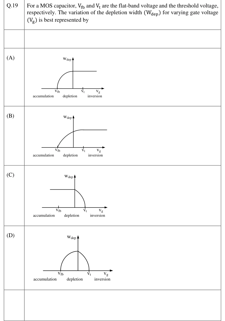
For a MOS capacitor, and are the flat-band voltage and the threshold voltage, respectively. The variation of the depletion width () for varying gate voltage () is best represented by

GATE 2023 EC question 19: Four candidate plots of W_dep (y-axis) vs V_g (x-axis), each x-axis marked with two ticks V_fb (left) and V_t (right), and…Tap to open full size
Figure from the GATE 2023 EC paper. It is part of the question.
Figure description

Four candidate plots of W_dep (y-axis) vs V_g (x-axis), each x-axis marked with two ticks V_fb (left) and V_t (right), and labelled below into three regions: accumulation (left of V_fb), depletion (between V_fb and V_t), inversion (right of V_t). (A) W_dep=0 left of a point left of V_fb, then a rising curve that saturates to a flat plateau before reaching V_t, plateau continues flat through and beyond V_t. (B) W_dep=0 up to V_fb, then rises smoothly from V_fb and saturates to a flat plateau right around V_t, staying flat for all V_g>V_t. (C) W_dep starts at a nonzero flat plateau for V_g<V_t (extending through accumulation and depletion) then curves down to zero at and beyond V_t. (D) W_dep=0 at V_fb and at V_t, rising to a single peak (arch/triangular shape) in between, zero again for V_g>V_t.

  1. (A)

    Figure — Wdep rises before Vfb and saturates to a plateau before Vt is reached (early saturation, offset from the marked voltages)

  2. (B)

    Figure — Wdep = 0 for Vg < Vfb, rises smoothly starting exactly at Vfb, and saturates to a constant plateau at Vg = Vt, remaining flat through inversion

  3. (C)

    Figure — Wdep starts at a constant nonzero value through accumulation and depletion, then decreases to zero at Vt and stays zero in inversion

  4. (D)

    Figure — Wdep = 0 in accumulation and inversion, rising to a single peak only inside the depletion region between Vfb and Vt (arch shape)

Answer and solution
GATE 2023 EC Q.19: answer and solution

GATE 2022 EC Q.20

GATE 2022 · ECQ.20 · 1 mark · MCQ

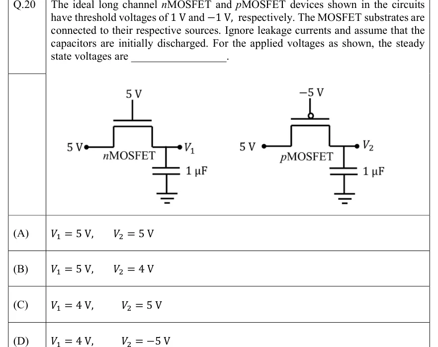
The ideal long channel MOSFET and MOSFET devices shown in the circuits have threshold voltages of 1 V and V, respectively. The MOSFET substrates are connected to their respective sources. Ignore leakage currents and assume that the capacitors are initially discharged. For the applied voltages as shown, the steady state voltages are ____________.

GATE 2022 EC question 20: Two separate circuits side by side.Tap to open full size
Figure from the GATE 2022 EC paper. It is part of the question.
Figure description

Two separate circuits side by side. LEFT circuit: an nMOSFET with its gate connected to a 5 V supply (gate terminal at top), its source (left terminal) connected to a '5 V' node, and its drain (right terminal) connected to node V1; a 1 uF capacitor connects node V1 to ground. RIGHT circuit: a pMOSFET with its gate connected to a '-5 V' supply (gate terminal at top, with a small circle indicating the PMOS gate bubble), its source (left terminal) connected to a '5 V' node, and its drain (right terminal) connected to node V2; a 1 uF capacitor connects node V2 to ground.

  1. (A)

    V1 = 5 V, V2 = 5 V

  2. (B)

    V1 = 5 V, V2 = 4 V

  3. (C)

    V1 = 4 V, V2 = 5 V

  4. (D)

    V1 = 4 V, V2 = -5 V

Answer and solution
GATE 2022 EC Q.20: answer and solution

GATE 2022 EC Q.34

GATE 2022 · ECQ.34 · 1 mark · NAT

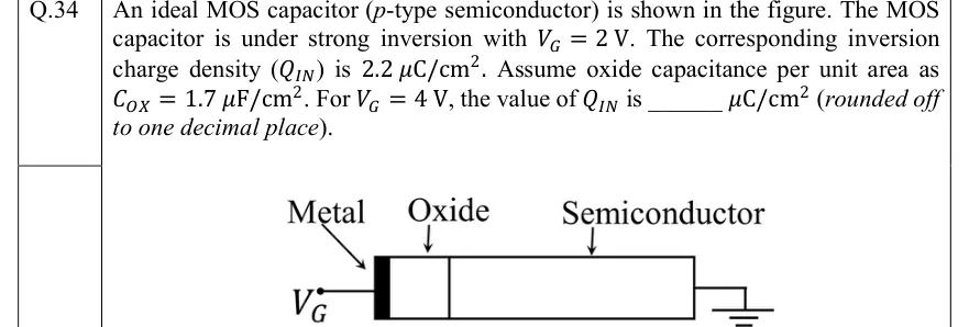
An ideal MOS capacitor (p-type semiconductor) is shown in the figure. The MOS capacitor is under strong inversion with V. The corresponding inversion charge density () is . Assume oxide capacitance per unit area as . For V, the value of is ______ (rounded off to one decimal place).

GATE 2022 EC question 34: Cross-section of an ideal MOS capacitor: from left to right, a thin black rectangular 'Metal' gate electrode, then a thin…Tap to open full size
Figure from the GATE 2022 EC paper. It is part of the question.
Figure description

Cross-section of an ideal MOS capacitor: from left to right, a thin black rectangular 'Metal' gate electrode, then a thin 'Oxide' layer, then a larger 'Semiconductor' (p-type) body on the right connected to ground (ground symbol at bottom right). An arrow labeled V_G with a dot (voltage source terminal) points to the metal gate from below-left, indicating the gate voltage applied to the metal electrode; the semiconductor body is grounded.

Answer and solution
GATE 2022 EC Q.34: answer and solution

GATE 2022 EC Q.40

GATE 2022 · ECQ.40 · 2 marks · MCQ

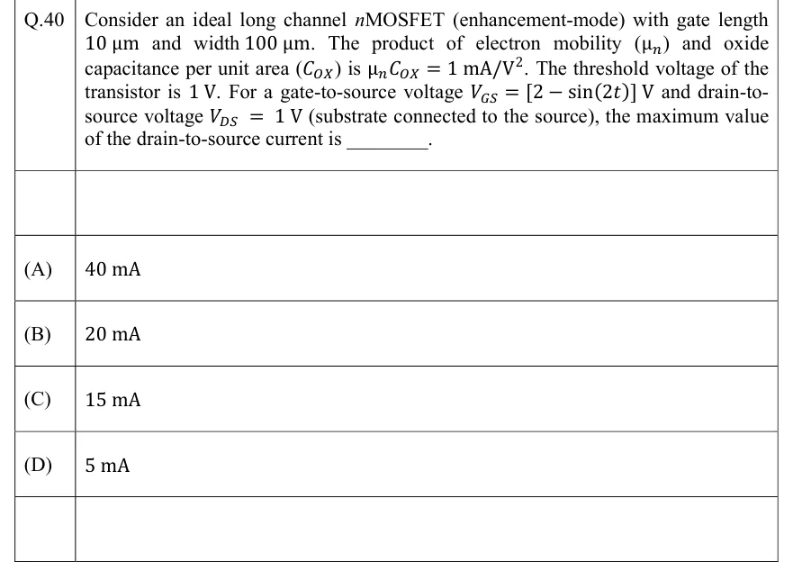
Consider an ideal long channel nMOSFET (enhancement-mode) with gate length 10 μm and width 100 μm. The product of electron mobility (μₙ) and oxide capacitance per unit area (C_OX) is μₙC_OX = 1 mA/V². The threshold voltage of the transistor is 1 V. For a gate-to-source voltage V_GS = [2 − sin(2t)] V and drain-to-source voltage V_DS = 1 V (substrate connected to the source), the maximum value of the drain-to-source current is ______.

  1. (A)

    40 mA

  2. (B)

    20 mA

  3. (C)

    15 mA

  4. (D)

    5 mA

Answer and solution
See the question in the paper
GATE 2022 EC Q.40: answer and solution

GATE 2020 EC Q.32

GATE 2020 · ECQ.32 · 2 marks · MCQ

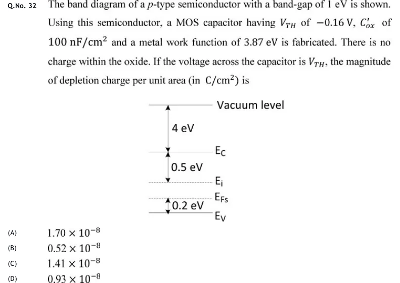
The band diagram of a p-type semiconductor with a band-gap of 1 eV is shown. Using this semiconductor, a MOS capacitor having of , of and a metal work function of is fabricated. There is no charge within the oxide. If the voltage across the capacitor is , the magnitude of depletion charge per unit area (in ) is

GATE 2020 EC question 32: Energy band diagram of a p-type semiconductor, vertical energy axis.Tap to open full size
Figure from the GATE 2020 EC paper. It is part of the question.
Figure description

Energy band diagram of a p-type semiconductor, vertical energy axis. Top to bottom: Vacuum level at top; a downward arrow of 4 eV from vacuum level to conduction band edge E_C (the electron affinity); below E_C a downward arrow of 0.5 eV to the intrinsic level E_i (dashed); below E_i the semiconductor Fermi level E_Fs (dashed), with an upward arrow of 0.2 eV from valence band edge E_V up to E_Fs; at the bottom, valence band edge E_V. Since band-gap is 1 eV and E_C - E_i = 0.5 eV, E_i - E_V is also 0.5 eV, so E_i - E_Fs = 0.5 - 0.2 = 0.3 eV.

  1. (A)

    1.70 x 10^-8

  2. (B)

    0.52 x 10^-8

  3. (C)

    1.41 x 10^-8

  4. (D)

    0.93 x 10^-8

Answer and solution
GATE 2020 EC Q.32: answer and solution

PRACTICE

5 questions to test yourself

PRACTICE 11 mark · MCQ

An NMOS capacitor (gate on p-type Si) has zero effective oxide charge () and a gate work function equal to the semiconductor work function. What is the flat-band voltage ?

  1. (A)

    0 V

  2. (B)

    Equal to

  3. (C)

    Equal to

  4. (D)

    Cannot be determined without

Answer and solution

Answer: (A)

  1. Flat-band voltage: .

  2. Equal work functions give , and is given.

  3. Both terms vanish, so .

PRACTICE 22 marks · NAT

An NMOS device has p-type body doping , oxide thickness , flat-band voltage and . Take at 300 K, , , , and . Find the threshold voltage in volts.

Answer and solution

Answer: (accepted range )

  1. .

  2. , so .

  3. . . Dividing by gives .

  4. .

PRACTICE 31 mark · MSQ

An ideal MOS capacitor is made on p-type silicon, with no source or drain regions. Its C-V curve is measured with a slow DC gate-voltage sweep, once with a low-frequency and once with a high-frequency small-signal test voltage. Which of the following statements are correct?

  1. (A)

    At low frequency, C rises back to nearly in strong inversion

  2. (B)

    At high frequency, C stays near its minimum value in strong inversion

  3. (C)

    At high frequency, C also rises back to in strong inversion

  4. (D)

    In accumulation, C is approximately at both low and high frequency

Answer and solution

Answer: (A), (B), (D)

  1. In strong inversion at low test frequency, minority carriers (electrons) are generated fast enough to follow the signal, so the inversion layer responds and C rises back towards . (A) is correct.

  2. At high test frequency, generation is too slow for the inversion charge to follow the signal, and no source or drain region can supply electrons. Only the depletion edge at responds, so C stays at ( in series with ). (B) is correct and (C) is incorrect.

  3. In accumulation, majority carriers (holes) respond at both frequencies, so in both cases. (D) is correct.

PRACTICE 41 mark · NAT

A long-channel NMOS transistor is biased in saturation with overdrive voltage and . Neglecting channel-length modulation, find the transconductance in .

Answer and solution

Answer: (accepted range )

  1. In saturation, .

  2. .

  3. . Check: , and .

PRACTICE 52 marks · MCQ

Under ideal constant-field scaling by a factor (all dimensions, the supply voltage and the threshold voltage scaled by ; doping scaled by ; long-channel square-law behaviour), how does the power density (power per unit chip area) change?

  1. (A)

    Stays constant

  2. (B)

    Increases by a factor of

  3. (C)

    Increases by a factor of

  4. (D)

    Decreases by a factor of

Answer and solution

Answer: (A)

  1. Constant-field scaling: ; ; . The internal electric fields stay the same.

  2. Current per device: . Here , is unchanged and , so .

  3. Power per device: .

  4. Area per device shrinks as , so power density . It is unchanged.

OFFICIAL GATE 2027 SYLLABUS WORDING

Copied from the GATE 2027 syllabus; see all 2027 syllabi.

GATE EC

MOS capacitor, MOSFET, scaling in MOSFETs

Preparing in Kolkata? IAE Academy's course for GATE ECE.