GATE 2026 EC Q.14
Consider carrier transport in a Zener diode in the breakdown region.
Which is the dominant transport mechanism for current flow in this case?
- (A)
Drift
- (B)
Diffusion
- (C)
Tunneling
- (D)
Ballistic transport

GATE EC
How a junction between p-type and n-type silicon builds a built-in potential and a depletion region, and how the depletion width, peak field and depletion capacitance depend on doping and bias. Covers how the ideal (Shockley) diode equation, the saturation current and the diffusion capacitance come from minority-carrier injection and storage, and how reverse breakdown by avalanche multiplication or Zener tunnelling is used in the Zener diode as a voltage reference and regulator. A short section compares the p-n junction with metal-semiconductor (Schottky and ohmic) contacts. Every formula states its conditions and sign convention.
6 previous-year questions · 5 solved · 4 practice questions
When p-type and n-type regions of the same semiconductor are joined, mobile carriers diffuse across the junction. The space charge they leave behind (ionized acceptors on the p-side, ionized donors on the n-side) builds an electric field, and diffusion stops when that field is strong enough to balance it. At equilibrium the Fermi level is flat across the structure, and this alignment is what fixes the built-in potential. Conventions used throughout:
The depletion approximation (no mobile carriers inside the depletion region, abrupt edges) is assumed.
BUILT-IN POTENTIAL
Holds at thermal equilibrium with complete ionization and non-degenerate doping ( well below the effective densities of states). and are the net acceptor and donor concentrations on the two sides. is positive: the n-side sits above the p-side. It cannot be read with a voltmeter across the diode, because the contact potentials at the metal contacts cancel it.
BUILT-IN POTENTIAL FROM CARRIER RATIOS
Equilibrium majority and minority concentrations on the two sides, with and . This is the same result as above, written with the mass-action law.
How the depletion region forms (teaching order)
Before contact: separate flat-band p and n regions with different Fermi levels.
On contact: electrons diffuse from n to p and holes from p to n, leaving fixed ionized dopant charge near the junction.
This space charge creates a built-in field pointing from n to p, which opposes further diffusion.
At equilibrium the drift and diffusion currents of each carrier cancel exactly: zero net current and a flat Fermi level.
The result is a depletion (space-charge) region with almost no mobile carriers, across which the full built-in potential is dropped.
DEPLETION WIDTH (STEP/ABRUPT JUNCTION)
For an abrupt (step) junction under the depletion approximation. It holds in reverse bias and in forward bias only while stays well below ; the approximation fails as . In reverse bias , so the bracket becomes and grows. ; for Si, , giving .
CHARGE BALANCE AND INDIVIDUAL DEPLETION WIDTHS
Charge neutrality: the ionized charge on the two sides is equal and opposite. The more lightly doped side always holds most of .
PEAK ELECTRIC FIELD (STEP JUNCTION)
The peak is at the metallurgical junction (). The field falls linearly to zero at each depletion edge, so the profile is a triangle whose area equals .
DEPLETION WIDTH (LINEARLY GRADED JUNCTION)
For a doping profile that changes linearly through the junction, where is the grading constant in . Here , compared with the square-root dependence of the step junction.
The depletion region acts like a parallel-plate capacitor whose plate separation is the bias-dependent width . It is a small-signal (incremental) capacitance : the change in depletion charge for a small change in bias. Since grows with reverse bias, falls as reverse bias increases. Varactor diodes use this voltage-tunable capacitance.
DEPLETION CAPACITANCE (GENERAL)
is the junction cross-sectional area and is the depletion width at the bias point. This holds for any doping profile as a small-signal capacitance.
DEPLETION CAPACITANCE VS BIAS
is the capacitance at zero bias. The grading exponent is for an abrupt junction and for a linearly graded one. In reverse bias , so the bracket is and . The formula applies in reverse bias and at small forward bias only; it wrongly diverges as .
1/C_J^2 VS REVERSE BIAS (ONE-SIDED ABRUPT JUNCTION)
is the doping of the lightly doped side. A plot of against is a straight line: its slope gives , and its intercept on the voltage axis is at .
EXAM TIP
For a strongly one-sided junction (for example ), , so the lighter doping sets both and . The relative error in the bracket is , which is 1% for a 100:1 ratio, so you can use the shortcut directly for a pn or np diode.
The applied bias injects minority carriers across the depletion region. They diffuse into the neutral regions and recombine over a diffusion length. The minority-carrier concentration at each depletion edge follows the law of the junction. Integrating the resulting diffusion currents at the depletion edges gives the ideal (Shockley) diode equation.
LAW OF THE JUNCTION
Minority-carrier concentrations at the n-side and p-side depletion edges. Valid for low-level injection, meaning the injected minority density stays well below the majority density.
IDEAL DIODE EQUATION
flows from p to n through the diode. is forward bias and is reverse bias. When in reverse bias, . Assumes low-level injection and no generation or recombination inside the depletion region.
DIODE EQUATION WITH IDEALITY FACTOR
when diffusion current dominates. approaches 2 when recombination in the depletion region dominates, which is typical of Si at low forward current. Use unless the question gives another value.
REVERSE SATURATION CURRENT (LONG-BASE DIODE)
and are the minority-carrier diffusion coefficients, with (Einstein relation). and are the diffusion lengths. This form holds when each neutral region is much longer than its diffusion length. In a short-base diode, replace and by the neutral-region widths.
EQUILIBRIUM MINORITY-CARRIER CONCENTRATIONS
is the equilibrium hole concentration on the n-side and the equilibrium electron concentration on the p-side. From the mass-action law, for non-degenerate doping.
SMALL-SIGNAL (DYNAMIC) RESISTANCE IN FORWARD BIAS
is the DC forward current at the bias point, with . For example, at 1 mA with at 300 K.
Temperature. and , so . For Si near 300 K ( eV) this is about per kelvin, so the ideal roughly doubles every 5 K.
In a practical Si diode the reverse current is usually dominated by generation current, which goes as rather than . Half the rate gives a doubling roughly every 9–10 K; this is where the often-quoted "doubles every 10°C" comes from.
At a fixed forward current, the forward voltage falls as temperature rises. The temperature coefficient is negative, typically about for Si; the exact value depends on the current.
The Shockley equation predicts a reverse current that saturates at . In real Si diodes at room temperature, carriers generated thermally inside the depletion region add a current proportional to . This generation current is usually larger than the ideal , and since grows with , it keeps rising slowly with reverse bias instead of saturating cleanly.
EXAM TIP
When a question gives at one temperature and asks for it at another, use whatever rule the question states: with the given , or a stated doubling temperature. Don't assume a fixed doubling interval unless the question gives one.
Under forward bias, excess minority carriers are stored in the neutral regions while they diffuse and recombine. The stored charge changes with , and this defines a diffusion capacitance. It matters only in forward bias and grows in proportion to the forward current. Unlike , it is negligible in reverse bias.
DIFFUSION CAPACITANCE (ONE-SIDED DIODE)
Charge-control result for a one-sided long-base diode in forward bias (). The stored charge is , where is the minority-carrier lifetime on the lightly doped (injected) side. In a short-base diode, replace by the transit time , where is the neutral n-region width. A full small-signal analysis of a long-base diode at low frequency gives half this value, ; use whichever form the question specifies.
One-sided junction (e.g. p$^+$n): what simplifies
Injection is essentially one-way: holes injected into the lightly doped n-side dominate, and electron injection into the heavily doped p-side is negligible.
(drop the term for the heavily doped side).
and are set almost entirely by the doping of the lightly doped side.
, using the hole lifetime on the n-side.
EXAM TIP
In reverse bias and at low forward bias, dominates the diode's small-signal capacitance. At the forward currents used in switching, dominates. The stored charge has to be removed before the diode can turn off, so the reverse-recovery (storage) time scales with . A fast-switching diode needs a short .
Under enough reverse bias every p–n junction breaks down and conducts heavily in the reverse direction. The two physical mechanisms are avalanche multiplication and Zener (band-to-band) tunnelling. Doping decides which one dominates, because it sets both the peak field and the depletion width at a given reverse voltage.
Avalanche vs Zener tunnelling
Property | Avalanche breakdown | Zener tunnelling |
|---|---|---|
Mechanism | Carriers accelerated by the field gain enough energy to impact-ionize lattice atoms; the new carriers ionize further, so the current multiplies | Heavy doping on both sides makes very narrow and the field very high (of order V/cm). Under reverse bias, filled valence-band states on the p-side line up with empty conduction-band states on the n-side, and electrons tunnel directly across |
Doping level | Lightly to moderately doped (at least one side) | Heavily doped on both sides |
Typical breakdown voltage (Si) | Higher, roughly above 6–7 V | Lower, roughly below 5 V; the two mechanisms coexist in between |
Knee of the I–V curve | Sharp | Softer, more gradual |
Temperature coefficient of | Positive: breakdown voltage rises with temperature | Negative: breakdown voltage falls with temperature, since decreases |
AVALANCHE BREAKDOWN VOLTAGE (ONE-SIDED ABRUPT JUNCTION)
is the doping of the lightly doped side. is the critical field for avalanche, a few V/cm in Si, and it changes only weakly with doping. is neglected next to . So : lighter doping gives a higher breakdown voltage.
The two temperature coefficients have opposite signs. Diodes that break down near the crossover (roughly 5–6 V in silicon) therefore have a net temperature coefficient close to zero, which makes them a good choice for stable voltage references.
The Zener diode as a device
A diode designed to operate continuously in reverse breakdown at a specified voltage . The name covers both mechanisms: low-voltage devices (below about 5 V in Si) break down by tunnelling and need heavy doping on both sides, while higher-voltage devices break down by avalanche.
In breakdown the current can change by orders of magnitude for a small change in voltage. This near-vertical part of the – curve is what makes it useful as a voltage reference or regulator.
It must be used with an external series resistor to limit the current; once breakdown starts, the device itself does not limit current.
It is rated by at a specified test current, by its dynamic resistance in breakdown (ideally small), by the minimum (knee) current needed for regulation, and by its maximum power .
ZENER PIECEWISE-LINEAR MODEL (IN BREAKDOWN)
is the reverse current, taken positive, with . is the knee voltage and the dynamic resistance. An ideal Zener has .
SHUNT REGULATOR: SERIES-RESISTOR LIMITS (IDEAL ZENER)
Supply feeds the Zener in parallel with the load through a series resistor . keeps the Zener in regulation in the worst case (lowest supply, highest load current). keeps the Zener current within its rating in the worst case (highest supply, lowest load current). Assumes .
EXAM TIP
First check that the Zener is actually in breakdown. With the Zener removed, the load voltage is . If that is below , the Zener is off and the output is just this divider voltage, not .
A metal on a semiconductor forms either a rectifying (Schottky) junction or a non-rectifying (ohmic) contact. Which one you get depends on the work-function difference and the doping. The band-bending logic is the same as for a p–n junction, with the metal taking the place of one doped region. The relations below are the ideal Schottky–Mott model, which ignores interface states; real barrier heights are often pinned by those states. Energies and work functions are in eV.
IDEAL SCHOTTKY BARRIER HEIGHT
is the metal work function and the semiconductor's electron affinity. is the barrier to electrons on n-type material and the barrier to holes on p-type material. On n-type, the built-in potential of the contact is , in volts.
SCHOTTKY DIODE THERMIONIC-EMISSION CURRENT
is the contact area, the effective Richardson constant, and the barrier height in volts (numerically equal to its value in eV). The prefactor is the saturation current, which replaces the diffusion-based of a p–n junction. For typical barrier heights it is several orders of magnitude larger than a comparable p–n junction's .
Rectifying or ohmic (ideal model)
Rectifying (Schottky), n-type: , the semiconductor work function. Electrons flow into the metal and the bands bend upward, leaving a barrier to electrons. For p-type the condition is reversed: .
Ohmic, n-type: . The bands bend down into electron accumulation, so electrons meet no barrier in either direction. For p-type the condition is .
Ohmic by tunnelling: heavily dope the semiconductor under the contact. The barrier becomes thin enough for carriers to tunnel through it freely whatever its height. This is the usual practical way ohmic contacts are made, since interface states often prevent the ideal work-function condition.
EXAM TIP
At the same moderate current, a silicon Schottky diode typically drops about 0.2–0.4 V, against about 0.6–0.7 V for a p–n diode. The reason is its much larger saturation current, which comes from the relatively small barrier. It is also a majority-carrier device, so it stores almost no minority charge and switches off quickly, with negligible reverse-recovery time.
WORKED EXAMPLE · EXAMPLE 1: BUILT-IN POTENTIAL AND DEPLETION WIDTH
A silicon step junction has and . Take , and , with zero applied bias. Find and the depletion width .
. and , so the ratio is .
, so .
Since , the junction is strongly one-sided: (error 0.1%).
.
. Multiplying by gives , and multiplying by gives .
, almost all of it on the lightly doped n-side.
Answer: and , essentially all on the n-side.
WORKED EXAMPLE · EXAMPLE 2: ZENER REGULATOR SERIES RESISTOR
A silicon Zener diode with (treat it as ideal, ) is fed from a 12 V source through a series resistor . The load draws a fixed 20 mA, and the Zener must carry at least 5 mA at all times to stay in regulation. Find the largest allowed , and the Zener's dissipation if the load is disconnected.
The current through must supply both the load and the minimum Zener current: .
The source and the regulated output fix the voltage across : .
is largest when the current is at its minimum: .
With and the load disconnected, all 25 mA flows through the Zener: . The Zener's power rating must be at least this.
Answer: . A larger resistor would starve the Zener of its minimum regulating current at full load. With no load, the Zener dissipates 155 mW.
WORKED EXAMPLE · EXAMPLE 3: DEPLETION CAPACITANCE UNDER REVERSE BIAS
An abrupt-junction diode has zero-bias capacitance and . Find at a reverse bias .
Abrupt junction, so , and reverse bias gives .
.
.
Answer: .
PREVIOUS-YEAR QUESTIONS
Try each question first, then open the answer. One shows the official answer only. We placed each question under a topic ourselves; the exam paper does not label topics.
See these papers in full: GATE ECE 2026 · GATE ECE 2025 · GATE ECE 2020 · GATE ECE 2018
Consider carrier transport in a Zener diode in the breakdown region.
Which is the dominant transport mechanism for current flow in this case?
Drift
Diffusion
Tunneling
Ballistic transport
Consider a p-n junction diode when it is forward biased with 2 V. Which of the following is/are the correct magnitude(s) of the energy difference between quasi Fermi-levels, in the n-side and in the p-side?
2 eV
1 eV
2 V
1 V
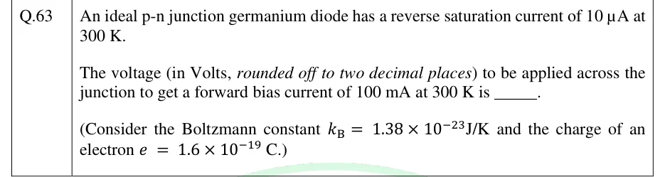
An ideal p-n junction germanium diode has a reverse saturation current of 10 μA at 300 K.
The voltage (in Volts, rounded off to two decimal places) to be applied across the junction to get a forward bias current of 100 mA at 300 K is ______.
(Consider the Boltzmann constant and the charge of an electron .)
A one-sided abrupt pn junction diode has a depletion capacitance of 50 pF at a reverse bias of 0.2 V. The plot of versus the applied voltage for this diode is a straight line as shown in the figure below. The slope of the plot is ____ .
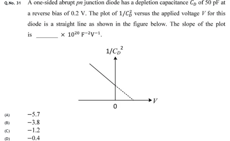 Tap to open full size
Axes: vertical axis labeled 1/C_D^2, horizontal axis labeled V, origin marked 0. A solid straight line with negative slope runs from the upper-left down to where it crosses the vertical (1/C_D^2) axis at a positive value; from that crossing point it continues as a dashed line with the same slope down to the right until it meets the horizontal V axis at a positive value of V (no numerical axis labels are printed).
-5.7
-3.8
-1.2
-0.4
Official answer: marks to all candidatesSource: Official answer key, GATE 2020 EC (IIT Delhi)
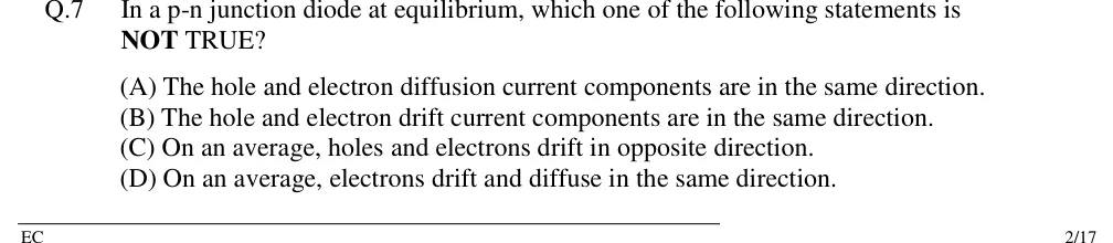
In a p-n junction diode at equilibrium, which one of the following statements is NOT TRUE?
The hole and electron diffusion current components are in the same direction.
The hole and electron drift current components are in the same direction.
On an average, holes and electrons drift in opposite direction.
On an average, electrons drift and diffuse in the same direction.
A p-n step junction diode with a contact potential of has a depletion width of at equilibrium. The forward voltage (in volts, correct to two decimal places) at which this width reduces to is ______.
PRACTICE
A silicon step p–n junction at 300 K has , and . Taking , the built-in potential is closest to:
0.35 V
0.64 V
0.90 V
1.10 V
Answer: (B)
and
The ratio is , and
In the junction above (), charge balance shows that the depletion region extends mainly into the:
p-side
n-side
Equally on both sides
Depends only on the applied bias sign
Answer: (B)
Charge balance gives
So : most of lies on the lightly doped side
Here the lightly doped side is the n-side
For a silicon p–n junction diode at 300 K, which of the following statements are correct?
increases with temperature because increases with temperature
Diffusion capacitance dominates over depletion capacitance under strong forward bias
Depletion capacitance decreases as reverse-bias magnitude increases
The peak electric field occurs at the neutral-region boundary, away from the junction
Answer: (A), (B), (C)
A: , and (proportional to ) rises steeply with , so increases with temperature. Correct.
B: under strong forward bias, the stored excess minority charge makes the diffusion capacitance (, growing with current) far larger than the depletion capacitance . Correct.
C: , and grows with reverse-bias magnitude, so falls as reverse bias increases. Correct.
D: false. In a step junction the peak field is at the metallurgical junction (), where the space-charge density changes sign. At the depletion edges, next to the neutral regions, the field is zero.
A one-sided (pn) silicon diode has reverse saturation current at 300 K (, ideality factor 1). Using , find the forward voltage (in volts) needed to reach .
Answer: (accepted range )
(the in the Shockley equation is negligible in forward bias)
OFFICIAL GATE 2027 SYLLABUS WORDING
Copied from the GATE 2027 syllabus; see all 2027 syllabi.
GATE EC
P-N junction, Zener diode
Preparing in Kolkata? IAE Academy's course for GATE ECE.