GATE 2025 EC Q.31
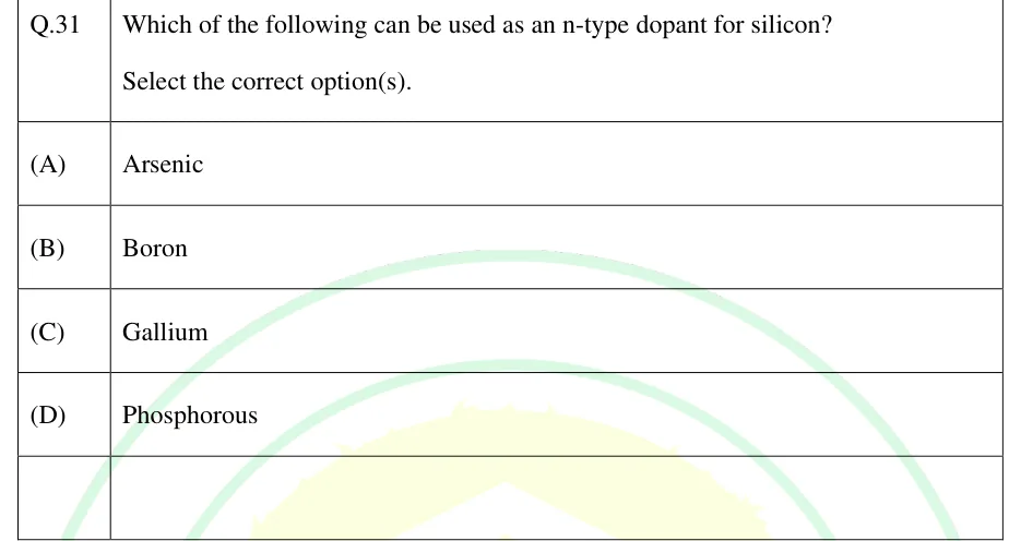
Which of the following can be used as an n-type dopant for silicon? Select the correct option(s).
- (A)
Arsenic
- (B)
Boron
- (C)
Gallium
- (D)
Phosphorous

GATE EC
Energy bands and carrier concentration covers how the discrete levels of isolated atoms broaden into a valence band and a conduction band separated by a forbidden gap , and how temperature and doping set the equilibrium electron and hole concentrations. The core results are Fermi–Dirac occupation and its Boltzmann approximation, and in terms of , and , the intrinsic concentration and its temperature dependence, the mass-action law , charge neutrality with compensated doping, the position of the Fermi level, and the direct/indirect band-gap distinction that governs light emission. Conventions: concentrations in cm, energies in eV, , at 300 K.
9 previous-year questions · 9 solved · 6 practice questions
When atoms are brought together to form a crystal, the electron wavefunctions of neighbouring atoms overlap and each discrete atomic level splits — as the Pauli exclusion principle requires — into as many closely spaced levels as there are atoms. With of order – atoms per cm (about in silicon) these levels are so close together that they form effectively continuous energy bands. In a semiconductor, the highest band that is completely filled at is the valence band (top edge ), and the next band above it, empty at 0 K, is the conduction band (bottom edge ). Between them lies the forbidden gap : a perfect crystal has no allowed electron states in this energy range.
Whether a material is a conductor, insulator or semiconductor is decided by (a) whether the highest occupied band is completely full or only partly full at , and (b) the size of the gap separating a full valence band from the empty conduction band.
A hole is an empty state in the otherwise full valence band. It behaves as a carrier of charge with its own effective mass, so electrons in the conduction band (concentration ) and holes in the valence band (concentration ) are treated as two separate carrier populations.
EXAM TIP
Band diagrams plot electron energy upward. is how far the Fermi level sits below the conduction-band edge, and is how far it sits above the valence-band edge. Keep this sign convention fixed whenever you solve for .
The size of the band gap (in eV) separates the three classes. A larger gap means far fewer carriers can be thermally excited across it, so intrinsic conduction falls sharply as increases.
Material | Band structure at 0 K | Typical (eV) | Conduction |
|---|---|---|---|
Conductor (metal) | Partially filled band, or overlapping valence and conduction bands | No gap | High; the carriers are already present, and conductivity falls as rises (more lattice scattering) |
Semiconductor | Valence band full, conduction band empty, moderate gap | Roughly – (at 300 K: Ge , Si , GaAs ) | Zero at 0 K (behaves as an insulator); rises steeply with as carriers are thermally generated |
Insulator | Valence band full, conduction band empty, large gap | Typically above about 4 (e.g. diamond , SiO ) | Negligible at ordinary temperatures |
EXAM TIP
In this simple band model a semiconductor and an insulator differ only in the size of , and the boundary between them is a convention, not a sharp line: wide-gap materials such as GaN () are used as semiconductors. Consequence: a semiconductor's resistance falls as temperature rises (negative temperature coefficient), while a metal's rises.
A pure (intrinsic) semiconductor has no impurities: every electron thermally excited into the conduction band leaves exactly one hole in the valence band, so the electron and hole concentrations are equal, . The probability that a state of energy is occupied by an electron at temperature is given by the Fermi–Dirac distribution, and the energy at which this probability equals is the Fermi level .
FERMI–DIRAC DISTRIBUTION
Probability that an allowed state at energy is occupied by an electron, in thermal equilibrium. . For any , . At , for and for .
PROBABILITY THAT A STATE IS EMPTY (HOLE OCCUPANCY)
Used for holes in the valence band; follows directly from .
When , the Fermi–Dirac function reduces to the Maxwell–Boltzmann tail . Likewise, for , . A semiconductor whose lies at least about below and at least about above is called non-degenerate, and the simple exponential expressions for and below hold only in that case. Very heavy doping can push close to or into a band (the degenerate case), where they fail.
DENSITY OF STATES NEAR THE CONDUCTION-BAND EDGE
Number of states per unit volume per unit energy for a parabolic band. has the same form with and for . The electron concentration is taken over the conduction band, which gives the expression below.
EQUILIBRIUM ELECTRON AND HOLE CONCENTRATIONS
Valid in thermal equilibrium for a non-degenerate semiconductor ( at least about from and from ), whatever the doping. and are the effective densities of states of the conduction and valence bands.
EFFECTIVE DENSITIES OF STATES
In SI units these come out in m; divide by for cm. Both scale as , so they depend on the carrier effective masses and rise with temperature. They are material properties, not constants: in a numerical problem, use the values given.
INTRINSIC CARRIER CONCENTRATION
Holds in thermal equilibrium, non-degenerate; . For silicon at the commonly used value is (some texts use ). depends on the material and the temperature, so always use the value the problem states.
TEMPERATURE DEPENDENCE OF $N_I$
This follows from , and the exponential factor dominates. Taking as constant, two temperatures are related by .
In an intrinsic sample sits at the intrinsic level . It is exactly at mid-gap only if (that is, ) or at . Otherwise it is displaced slightly toward the band with the smaller effective mass (smaller density of states).
INTRINSIC FERMI LEVEL
Obtained by setting in the Boltzmann expressions. If , lies slightly above mid-gap. The shift is of order , small compared with .
CARRIER CONCENTRATIONS REFERRED TO $E_I$
Equivalent to the , forms and valid under the same conditions (equilibrium, non-degenerate, any doping). Multiplying the two gives directly.
Adding controlled impurities (doping) changes the carrier concentrations by orders of magnitude without changing . A donor (a Group V atom such as P or As in Si) introduces a level just below , a few tens of meV below it in Si. Its extra electron is easily ionised into the conduction band, making the material n-type. An acceptor (a Group III atom such as B or Ga in Si) introduces a level just above . It captures an electron from the valence band and leaves a hole, making the material p-type. Electrons are the majority carriers in n-type material and holes are the majority in p-type; the other carrier in each case is the minority carrier.
Identify the dopant concentrations (donors/cm) and (acceptors/cm). Take both as fully ionised at room temperature unless the problem says otherwise.
Find the majority-carrier concentration from charge neutrality (Section 5). If both dopants are present (compensation), use the net doping , not alone.
The approximation (or ) is valid only when . If they are comparable, for example at high temperature, use the exact quadratic solution in Section 5.
Find the minority-carrier concentration from the mass-action law, or .
Locate from the majority-carrier concentration using the formulas below.
FERMI LEVEL POSITION, N-TYPE
From the Boltzmann expressions; non-degenerate, equilibrium. lies above when .
FERMI LEVEL POSITION, P-TYPE
From the Boltzmann expressions; non-degenerate, equilibrium. lies below when .
WORKED EXAMPLE
A silicon sample at 300 K is doped with donors (fully ionised, no acceptors). Take and . Where is relative to ?
, so .
.
.
.
Answer: lies about above (toward ).
Because more donors raise , the formulas above show that a higher moves closer to (further above ). Symmetrically, a higher moves closer to . The change is only logarithmic: each tenfold increase in doping moves by at 300 K. In a non-degenerate semiconductor stays inside the gap, at least about from either band edge.
MASS-ACTION LAW
Holds in thermal equilibrium in a non-degenerate semiconductor, doped or undoped, with evaluated at the same temperature. It does not hold under illumination or carrier injection (non-equilibrium).
CHARGE NEUTRALITY (GENERAL)
Total negative charge equals total positive charge in the bulk, where and are the ionised acceptor and donor concentrations. With full ionisation, and .
COMPENSATED DOPING (FULL IONISATION)
Combine with to solve for and . If , the material is n-type when (then ) and p-type when (then ); the minority carrier follows from mass action.
EXACT EQUILIBRIUM SOLUTION ($N_D > N_A$)
This is the positive root of (full ionisation, non-degenerate). For swap the roles: . Needed whenever is not much larger than . With it gives .
WORKED EXAMPLE
A silicon sample is doped with phosphorus atoms and no acceptors, fully ionised, at 300 K where . Find and .
, so neutrality gives .
Since , , so (majority carrier).
Mass action gives the minority carrier: .
.
Answer: , (n-type).
WORKED EXAMPLE
Another silicon sample is doped with both donors and acceptors (compensated doping), both fully ionised, at 300 K (). Find the majority- and minority-carrier concentrations.
Net doping: , so the material is n-type.
Since : .
Mass action gives the minority holes: .
.
Answer: (majority, electrons), (minority, holes).
EXAM TIP
In compensated material, use the net doping for the majority carrier, never or alone. Compensation cancels only the ionised charge in the neutrality equation. All ionised impurities still scatter carriers, so a compensated sample does not regain the mobility of a lightly doped one.
rises steeply with . The exponential factor dominates the weaker factor, and itself also decreases slightly as rises, which adds to the increase. A doped sample passes through three ranges as rises. At low it is in freeze-out: not all dopants are ionised, so . Over a wide middle range it is in the extrinsic (saturation) range: , essentially constant with , which is the normal operating range for devices. At high enough , grows until it is comparable to and the sample enters the intrinsic range, where doping no longer controls the carrier concentration.
THERMAL VOLTAGE
at , with and . Equivalently at 300 K, so an energy difference in eV divided by in eV gives the dimensionless exponent in the Boltzmann expressions directly.
As rises from the extrinsic range toward the intrinsic range, the Fermi level of a doped sample moves away from (n-type) or (p-type) and approaches . The reason: grows rapidly while the dopant concentration stays fixed, so (or ) falls toward 1, and falls toward zero.
Band structure is drawn on an energy versus crystal-momentum (–) diagram. In a direct band-gap material the conduction-band minimum and the valence-band maximum occur at the same ; in an indirect band-gap material they occur at different . The curvature of the band near an edge sets the carrier effective mass.
EFFECTIVE MASS FROM THE $E$–$K$ DIAGRAM
Evaluated at the band edge, with . A sharply curved band gives a small effective mass. For a parabolic conduction band, .
Property | Direct gap (e.g. GaAs, InP) | Indirect gap (e.g. Si, Ge, GaP) |
|---|---|---|
Band extrema in -space | Same | Different |
Band-to-band recombination | Energy carried off by a photon; the photon's momentum is negligible and no momentum change is needed | A phonon (lattice vibration) must also be emitted or absorbed to supply the difference in crystal momentum |
Radiative recombination efficiency | High | Low; most recombination is non-radiative, through defect (trap) levels in the gap |
Optical absorption just above | Strong | Weak (phonon-assisted); becomes strong only at higher photon energies |
Typical use | LEDs, laser diodes | Transistors, ICs, and also photodetectors and solar cells; not used as efficient light emitters |
BAND-GAP WAVELENGTH
The wavelength of a photon of energy . It gives the approximate emission wavelength of band-to-band recombination and the longest wavelength (cut-off) the material absorbs band-to-band. Uses .
WORKED EXAMPLE
Estimate the emission wavelength of a GaAs LED, taking .
with in eV and in m.
.
Answer: (about 873 nm, near-infrared).
EXAM TIP
The causal chain to know: indirect gap → band-to-band recombination needs a phonon → radiative recombination is improbable → poor light emitter. Silicon is a poor LED material because its gap is indirect, not because of the size of its gap.
PREVIOUS-YEAR QUESTIONS
Try each question first, then open the answer. We placed each question under a topic ourselves; the exam paper does not label topics.
See these papers in full: GATE ECE 2025 · GATE ECE 2024 · GATE ECE 2023 · GATE ECE 2022 · GATE ECE 2020 · GATE ECE 2018
Which of the following can be used as an n-type dopant for silicon? Select the correct option(s).
Arsenic
Boron
Gallium
Phosphorous
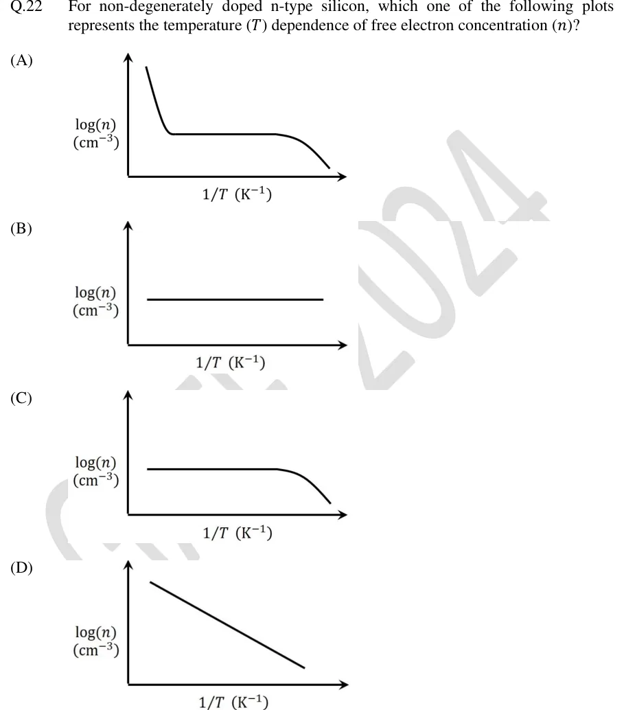
For non-degenerately doped n-type silicon, which one of the following plots represents the temperature () dependence of free electron concentration ()?
 Tap to open full size
Four small plots, each with axes log (n) (cm^-3) on the vertical axis and 1/T (K^-1) on the horizontal axis (increasing rightward, so low 1/T = high T is on the left and high 1/T = low T is on the right). (A): curve starts high near the top-left, drops steeply, levels into a flat horizontal plateau across the middle, then drops steeply again near the right end (three regions: intrinsic decrease, extrinsic plateau, freeze-out decrease). (B): a single flat horizontal line segment across the middle of the plot (constant log (n), no rise or fall shown). (C): a flat horizontal plateau starting from the left that curves downward only near the right end (plateau plus one drop, no left-side intrinsic decrease). (D): a single straight line with constant negative slope running from upper-left to lower-right (monotonic decrease, no plateau).
Figure — plot showing (left to right): a decreasing curve from high , then a flat plateau, then another decreasing curve near the right end (three-region S-shaped curve)
Figure — plot showing a single flat horizontal line (constant across the whole range)
Figure — plot showing a flat plateau on the left that bends downward only near the right end (two-region curve, no intrinsic rise on the left)
Figure — plot showing a single straight line with constant negative slope from upper-left to lower-right (simple monotonic decrease)
A non-degenerate n-type semiconductor has 5% neutral dopant atoms. Its Fermi level is located at 0.25 eV below the conduction band () and the donor energy level () has a degeneracy of 2. Assuming the thermal voltage to be 20 mV, the difference between and (in eV, rounded off to two decimal places) is ____.
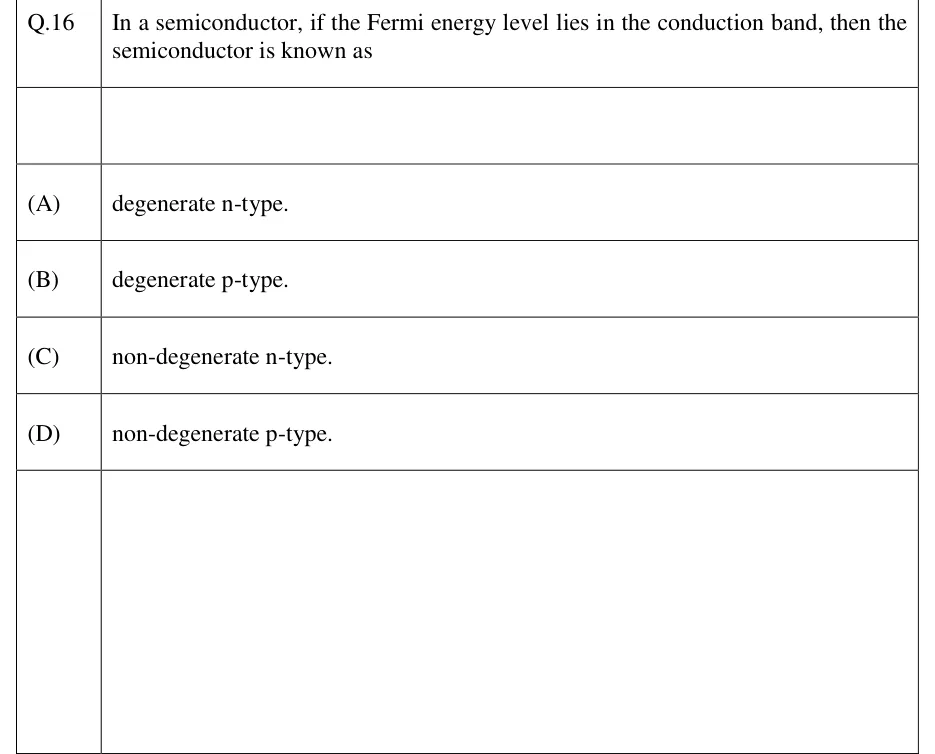
In a semiconductor, if the Fermi energy level lies in the conduction band, then the semiconductor is known as
degenerate n-type.
degenerate p-type.
non-degenerate n-type.
non-degenerate p-type.
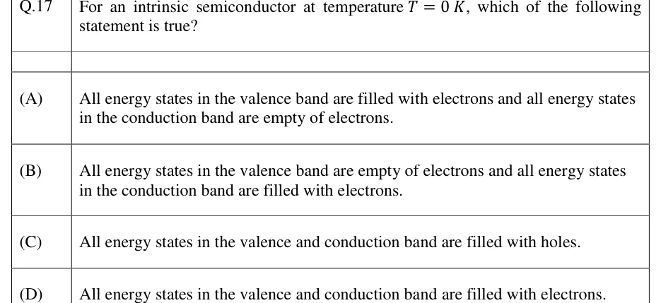
For an intrinsic semiconductor at temperature , which of the following statement is true?
All energy states in the valence band are filled with electrons and all energy states in the conduction band are empty of electrons.
All energy states in the valence band are empty of electrons and all energy states in the conduction band are filled with electrons.
All energy states in the valence and conduction band are filled with holes.
All energy states in the valence and conduction band are filled with electrons.
In a semiconductor device, the Fermi-energy level is 0.35 eV above the valence band energy. The effective density of states in the valence band at is . The thermal equilibrium hole concentration in silicon at 400 K is _______ (rounded off to two decimal places). Given kT at 300 K is 0.026 eV.
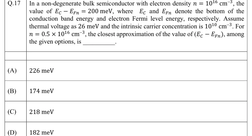
In a non-degenerate bulk semiconductor with electron density , the value of , where and denote the bottom of the conduction band energy and electron Fermi level energy, respectively. Assume thermal voltage as 26 meV and the intrinsic carrier concentration is . For , the closest approximation of the value of , among the given options, is ____.
226 meV
174 meV
218 meV
182 meV
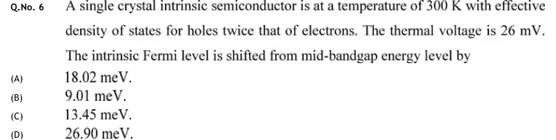
A single crystal intrinsic semiconductor is at a temperature of 300 K with effective density of states for holes twice that of electrons. The thermal voltage is 26 mV. The intrinsic Fermi level is shifted from mid-bandgap energy level by
18.02 meV.
9.01 meV.
13.45 meV.
26.90 meV.
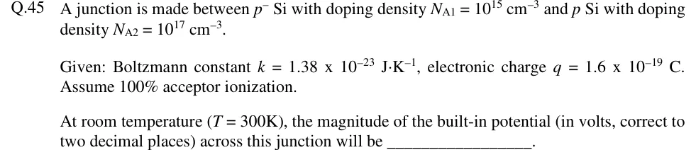
A junction is made between Si with doping density and Si with doping density .
Given: Boltzmann constant , electronic charge . Assume 100% acceptor ionization.
At room temperature (), the magnitude of the built-in potential (in volts, correct to two decimal places) across this junction will be ____.
PRACTICE
In an indirect band-gap semiconductor, radiative (photon-emitting) recombination of an electron–hole pair across the band gap necessarily also requires:
Nothing beyond the photon; energy conservation alone suffices
A phonon, to conserve crystal momentum in addition to the photon carrying away the energy
A second photon of equal and opposite momentum
The electron and hole to have equal effective mass
Answer: (B)
In an indirect-gap material the conduction-band minimum and the valence-band maximum lie at different crystal momentum .
A photon of energy near carries negligible momentum compared with this difference, so the photon alone cannot conserve momentum.
A phonon supplies or absorbs the momentum difference. The photon carries away the energy, which is minus or plus the small phonon energy. Both must take part in the same event.
Hence B. Because this process involves three particles, it is much less probable than direct-gap recombination.
An n-type silicon sample is in the extrinsic (saturation) range at moderate temperature. Its temperature is then raised further toward the intrinsic range, with the doping unchanged. Over this rise, the Fermi level , measured relative to the intrinsic level :
Moves further away from , toward
Moves toward
Stays exactly fixed at its extrinsic-range position
Jumps discontinuously to
Answer: (B)
In equilibrium, .
With full ionisation, . In the extrinsic range , so and lies well above .
As rises, grows rapidly (the factor) while is fixed, so falls toward 1 and falls toward 0.
So decreases and moves toward : option B.
Which of the following statements about the effective densities of states and are correct?
depends on the conduction-band electron effective mass , and on the valence-band hole effective mass
and are independent of temperature
and increase with temperature approximately as
and depend on the applied bias across the sample, not on the material
Answer: (A), (C)
and , so A and C are correct.
B is false: both scale as .
D is false: and are material properties (effective mass) that also depend on temperature. They do not depend on an applied bias.
A silicon sample is doped with donors and no acceptors, fully ionised, at where . Calculate the equilibrium minority-carrier (hole) concentration in cm.
Answer: (accepted range )
Since , the sample is n-type and .
Apply the mass-action law: .
.
.
A silicon sample at is compensation-doped with donors and acceptors, both fully ionised. Take and . Calculate in eV (positive if lies above ).
Answer: (accepted range )
Net doping: , so the material is n-type.
Since , . (Check: , negligible.)
.
, so .
Silicon has a band gap at 300 K. Using , calculate the longest wavelength (in m) of light that can generate electron–hole pairs by band-to-band absorption in silicon.
Answer: (accepted range )
Band-to-band absorption needs a photon energy of at least , so the cut-off wavelength is .
.
OFFICIAL GATE 2027 SYLLABUS WORDING
Copied from the GATE 2027 syllabus; see all 2027 syllabi.
GATE EC
Formation of energy bands in solids, energy bands in intrinsic and extrinsic semiconductors, equilibrium carrier concentration, direct and indirect band-gap semiconductors
Preparing in Kolkata? IAE Academy's course for GATE ECE.