
The logic gates shown in the digital circuit below use strong pull-down nMOS transistors for LOW logic level at the outputs. When the pull-downs are off, high-value resistors set the output logic levels to HIGH (i.e. the pull-ups are weak). Note that some nodes are intentionally shorted to implement "wired logic". Such shorted nodes will be HIGH only if the outputs of all the gates whose outputs are shorted are HIGH.
[Figure]
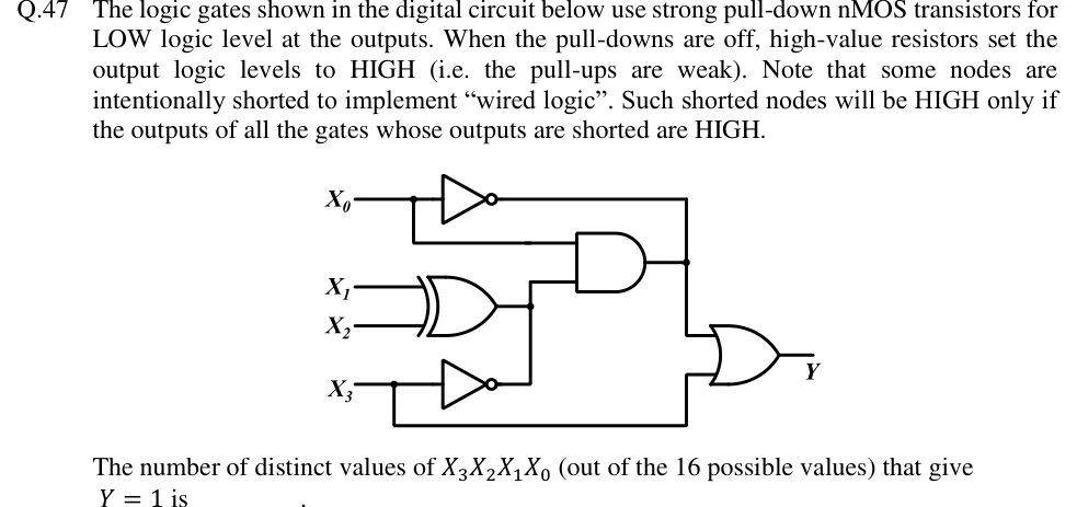
The number of distinct values of (out of the 16 possible values) that give is ________.
 Tap to open full size
Figure description
Inputs X0, X1, X2, X3 on the left; output Y on the right. (1) X0 feeds a NOT gate; a junction on the X0 line before the NOT also carries X0 directly to the TOP input of a 2-input AND gate. (2) X1 and X2 feed a 2-input XOR gate. (3) X3 feeds a second NOT gate; a junction on the X3 line before that NOT runs a wire along the bottom of the drawing to the BOTTOM input of a 2-input OR gate. (4) The XOR output goes to a junction; from it a wire goes up to the BOTTOM input of the AND gate and down to the output of the X3 NOT gate, so the XOR output and the output of NOT(X3) are shorted together (wired node). (5) The output of NOT(X0) runs right and then down to a junction at the AND gate's output, so the output of NOT(X0) and the AND output are shorted together (wired node). That wired node runs down to the TOP input of the OR gate. (6) The OR gate output is Y.