
IAE Academy

GATE 2025 EC Q.62: solution and answer

GATE 2025 · ECQ.62 · 2 marks · NAT

In the circuit shown below, the AND gate has a propagation delay of 1 ns. The edge-triggered flip-flops have a set-up time of 2 ns, a hold-time of 0 ns, and a clock-to-Q delay of 2 ns.

The maximum clock frequency (in MHz, rounded off to the nearest integer) such that there are no setup violations is ________.
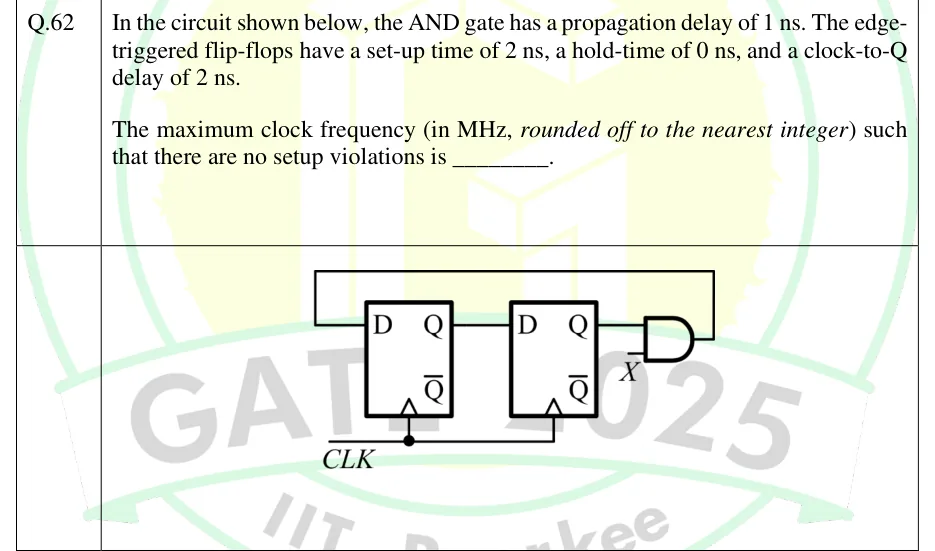
GATE 2025 EC question 62: Two edge-triggered D flip-flops, FF1 (left) and FF2 (right), each drawn with outputs Q and Q and a clock input marked with…Tap to open full size
Figure from the GATE 2025 EC paper. It is part of the question.
Figure description

Two edge-triggered D flip-flops, FF1 (left) and FF2 (right), each drawn with outputs Q and Q and a clock input marked with the edge-trigger triangle. A common line CLK drives the clock inputs of both flip-flops. Q of FF1 is wired directly to D of FF2. Q of FF2 feeds one input of a 2-input AND gate; the other AND input is an external signal X. The AND gate output loops back along the top of the figure to D of FF1. The Q outputs of both flip-flops are unconnected.

Answer and solution

ANSWER

The maximum clock frequency with no set-up violations is 200 MHz. The limiting path is FF2 → AND → FF1, which needs .

Official answer: 200Source: Official answer key, GATE 2025 EC (IIT Roorkee)

  1. Both flip-flops are clocked by the same CLK edge, so there are two flip-flop-to-flip-flop paths to check: FF1 → FF2 (a direct wire from Q of FF1 to D of FF2), and FF2 → AND gate → FF1 (the feedback path from Q of FF2, through the AND gate, back to D of FF1).

  2. For any register-to-register path, the data launched at one clock edge must settle at the next flip-flop's D input at least one set-up time before the following edge: .

  3. Path FF1 → FF2 has no logic in between: .

  4. Path FF2 → AND → FF1 passes through the AND gate: .

  5. The clock has to satisfy the slower path, so .

  6. The hold time (0 ns) only enters hold checks, not the set-up-limited maximum frequency. The external input has no timing given, so it is taken to be stable in time and does not limit the clock.

KEY IDEA

Check every path from one flip-flop to the next with . The path with the most logic in it (here the feedback loop through the AND gate) sets the minimum clock period, and .

WATCH OUT FOR

One mistake is checking only the direct FF1 → FF2 wire, which gives 4 ns and 250 MHz. Another is adding the hold time into the set-up equation, or adding the delays of both paths together (2 + 2 + 1 + 2 + 2 = 9 ns) as if the data had to cross both flip-flops in one clock cycle.

From the GATE 2025 EC paper. Every question of this paper · Download the full paper · All 30 Sequential questions, with notes

More Sequential questions