
IAE Academy

GATE 2024 IN Q.42: solution and answer

GATE 2024 · INQ.42 · 2 marks · MCQ

In the figure shown, the positive edge triggered D flip-flops are initially reset to Q = 0. The logic gates and the multiplexers have no propagation delay. After reset, a train of clock pulses (CLK) are applied. The logic-states of the inputs DIN, S and the clock pulses are also shown in the figure. Assuming no timing violations, the sequence of output Y from the 3rd clock to the 5th clock, is
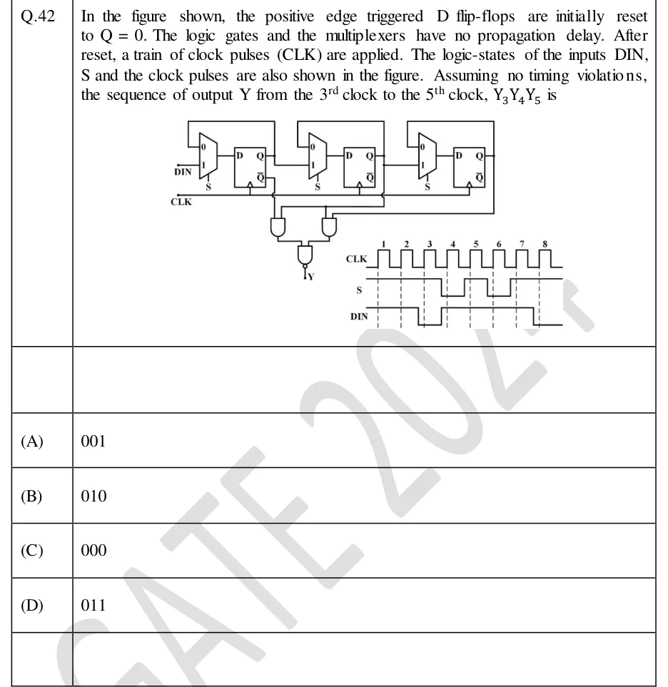
GATE 2024 IN question 42: Circuit: three identical stages, each a 2:1 MUX (inputs labelled 0 on top and 1 below, select line S common to all three)…Tap to open full size
Figure from the GATE 2024 IN paper. It is part of the question.
Figure description

Circuit: three identical stages, each a 2:1 MUX (inputs labelled 0 on top and 1 below, select line S common to all three) whose output drives the D input of a positive-edge-triggered D flip-flop; all three clock inputs are tied to the common CLK line. Stage 1: MUX input 0 = Q1 (fed back from its own Q), MUX input 1 = DIN. Stage 2: MUX input 0 = Q2 (own feedback), MUX input 1 = Q1. Stage 3: MUX input 0 = Q3 (own feedback), MUX input 1 = Q2. So S = 1 shifts right (DIN -> Q1 -> Q2 -> Q3) and S = 0 holds. Output logic: left 2-input AND gate has inputs Q̄1 (complement output of FF1) and Q2; right 2-input AND gate has inputs Q2 and Q3; both AND outputs go to a 2-input NAND gate whose output is Y. Q̄2 and Q̄3 are unconnected. Timing diagram: CLK shows 8 pulses numbered 1 to 8, dashed vertical lines at each rising edge. S: high from the start through rising edge 3, goes low between edges 3 and 4, back high between edges 4 and 5, low between edges 5 and 6, high between edges 6 and 7 and stays high through edge 8 (S at edges 1-8 = 1,1,1,0,1,0,1,1). DIN: high through edge 2, goes low between edges 2 and 3, goes high between edges 3 and 4, stays high through edge 7, goes low between edges 7 and 8 (DIN at edges 1-8 = 1,1,0,1,1,1,1,0).

  1. (A)

    001

  2. (B)

    010

  3. (C)

    000

  4. (D)

    011

Answer and solution

ANSWER

, option (A). The register goes , holds at on clock 4 (S = 0), then shifts to on clock 5. Here , which is 0 only in state 011.

Official answer: ASource: Official answer key, GATE 2024 IN (IISc Bengaluru)

  1. Read the MUX wiring. In each stage the 2:1 MUX drives the D input, with input 0 on top and input 1 below: , where input 1 is DIN, and for stages 1, 2 and 3. So shifts right () and holds the state, because each flip-flop reloads its own .

  2. Output logic (overline = complement): the left AND gate takes and , the right AND gate takes and , and both feed a NAND gate: So only in the state , and in every other state.

  3. Sample S and DIN at each rising edge. A positive-edge D flip-flop stores whatever is on D at the instant of the edge. From the timing diagram, S falls just after edge 3 and DIN rises just after edge 3, so at edges 1 to 5: and .

  4. Step through the states, starting from the reset state . Edge 1 (, DIN ): shift gives . Edge 2 (, DIN ): . Edge 3 (, DIN ): , so .

  5. Edge 4 (): every flip-flop reloads its own output, so the state stays . Edge 5 (, DIN ): , old , old , so .

  6. Evaluate Y after each clock. After clock 3 the state is , so and . After clock 4 the state is still , so . After clock 5 the state is , so , the product is and .

  7. Therefore , which is option (A).

KEY IDEA

Each MUX in front of a D flip-flop picks between holding and shifting. With each stage loads the stage to its left (DIN for stage 1), so the circuit is a right-shift register. With each stage reloads its own and nothing changes. The NAND of the two AND terms reduces to , so you only need to find when the register sits in state 011. Take S and DIN at the instant of each rising edge.

WATCH OUT FOR

The usual slip is to miss the hold on clock 4. S is 0 at that edge, but students often shift DIN = 1 in anyway, which gives states 011, 101, 110 and , the trap option (D). A second slip is reading S or DIN just after an edge instead of at it. Both change shortly after edge 3, so at edge 3 they are still S = 1 and DIN = 0. A third is misreading the left AND input as when the wire actually comes from .

From the GATE 2024 IN paper. Every question of this paper · Download the full paper · All 30 Sequential questions, with notes

More Sequential questions