
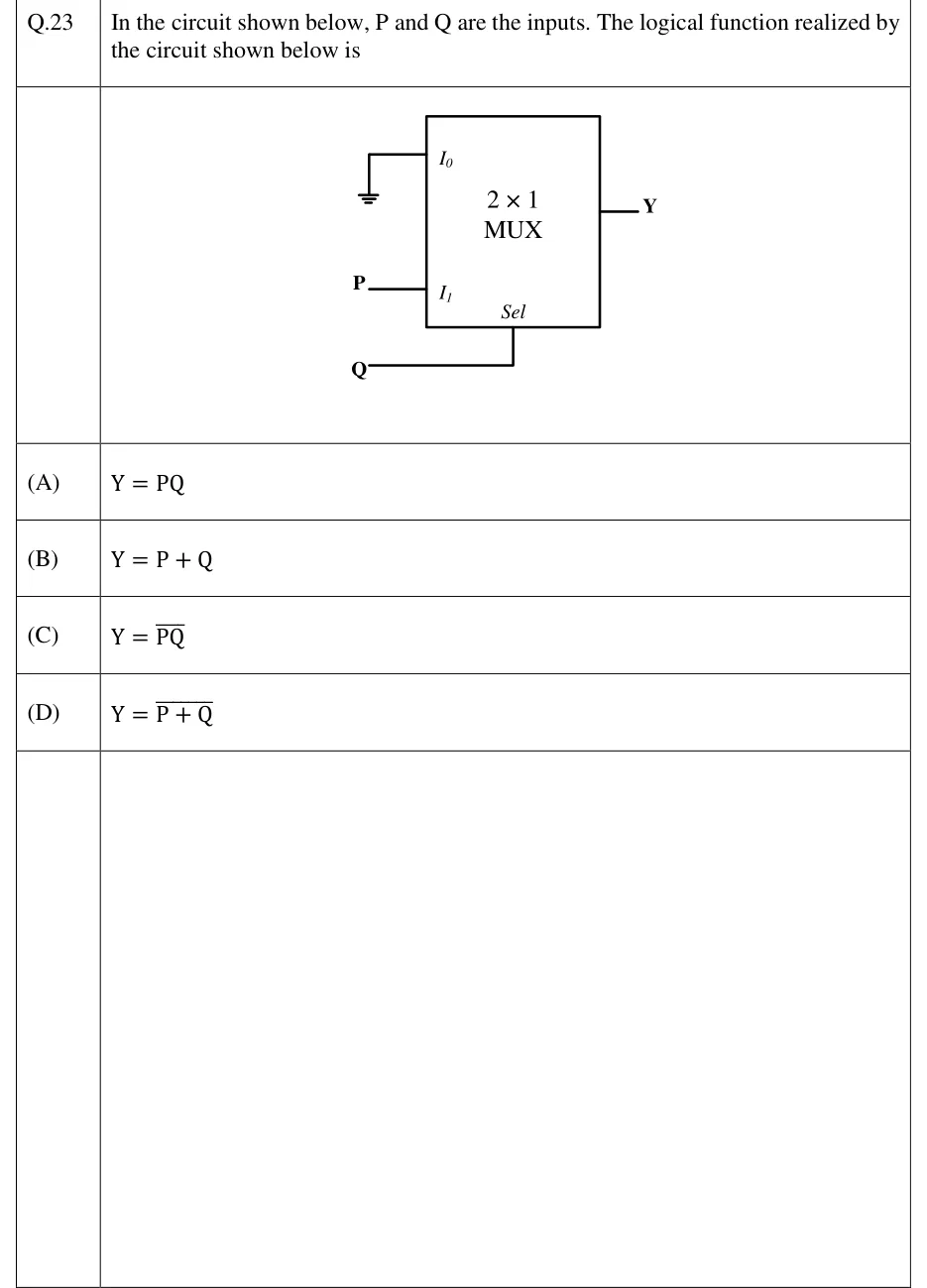
In the circuit shown below, P and Q are the inputs. The logical function realized by the circuit shown below is
 Tap to open full size
Figure description
A single 2 × 1 MUX block with output Y on the right. Data input I_0 is tied to ground (logic 0). Data input I_1 is driven by input P. The select line (Sel), entering from the bottom of the block, is driven by input Q. There are no other gates.
- (A)
- (B)
- (C)
- (D)