
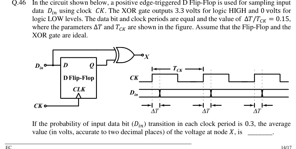
In the circuit shown below, a positive edge-triggered D Flip-Flop is used for sampling input data using clock . The XOR gate outputs 3.3 volts for logic HIGH and 0 volts for logic LOW levels. The data bit and clock periods are equal and the value of , where the parameters and are shown in the figure. Assume that the Flip-Flop and the XOR gate are ideal.
If the probability of input data bit () transition in each clock period is 0.3, the average value (in volts, accurate to two decimal places) of the voltage at node , is ______.
 Tap to open full size
Figure description
Circuit (left): input terminal D_in feeds the D input of a D Flip-Flop; the same D_in node also branches up and over to the first (upper) input of a 2-input XOR gate. The flip-flop output Q goes to the second (lower) input of the XOR gate. The XOR output is node X. Input terminal CK drives the flip-flop's CLK input (edge-triggered, marked with a triangle). Timing diagram (right): CK is a square wave with period T_CK (marked between two successive rising edges), about 50% duty cycle; three rising edges are shown. D_in is drawn as a data-eye waveform (two parallel lines with crossovers) whose transitions (crossovers) occur a delay Δ T AFTER each rising edge of CK; the Δ T interval is marked between each rising edge (dashed line) and the following D_in crossover (dashed line), three times. The data bit period equals T_CK.