
IAE Academy

GATE 2018 EC Q.2: solution and answer

GATE 2018 · ECQ.2 · 1 mark · MCQ

In the circuit shown below, the op-amp is ideal and Zener voltage of the diode is 2.5 volts. At the input, unit step voltage is applied, i.e. volts. Also, at , the voltage across each of the capacitors is zero.

The time , in milliseconds, at which the output voltage crosses is
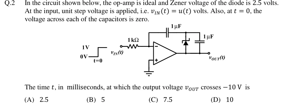
GATE 2018 EC question 2: Inverting integrator-type circuit with an ideal op-amp.Tap to open full size
Figure from the GATE 2018 EC paper. It is part of the question.
Figure description

Inverting integrator-type circuit with an ideal op-amp. Input: a unit step waveform (0 V before t = 0, 1 V after t = 0) is applied as v_IN(t) through a 1 kΩ resistor to the inverting (−) input. The non-inverting (+) input is grounded. Feedback network from the inverting input node to the op-amp output: a 1 µF capacitor (C1) connected along the top wire from the inverting-input node to a node X; from node X down to the output line there are two elements in parallel: a Zener diode (cathode at node X on top, anode at the output line below, triangle pointing up) and a second 1 µF capacitor (C2). So the feedback is C1 in series with (Zener || C2). The output line continues to the right as v_OUT(t). Both capacitors are uncharged at t = 0; Zener voltage 2.5 V.

  1. (A)

    2.5

  2. (B)

    5

  3. (C)

    7.5

  4. (D)

    10

Answer and solution

ANSWER

The output crosses at , which is option (C).

Official answer: CSource: Official answer key, GATE 2018 EC (IIT Guwahati)

  1. Assumptions. The op-amp is ideal, so the inputs form a virtual short, , and no current enters either input. No supply rails are given, so the output is taken as unsaturated. The feedback network is in series with the parallel pair (Zener ). The Zener's cathode is at the node between the capacitors and its anode is at the output. ( and are our labels; the figure prints only on each.)

  2. Input current for . With the inverting node at virtual ground, Ohm's law gives . None of it enters the op-amp, so this constant current flows through the feedback network towards the output.

  3. Phase 1 (Zener off). The same current charges and in series, . Both capacitors start uncharged, so

  4. When the Zener breaks down. The voltage across , which is also the voltage across the Zener, is . Current flows from the middle node through to the output, so the middle node (the cathode) is the positive side. The Zener is therefore reverse-biased and carries no current until , which happens at . At that moment , so the output has not yet reached .

  5. Phase 2 (Zener in breakdown). The Zener holds at , so takes no more current and the Zener carries the whole 1 mA. Only keeps charging, and it has been carrying since : .

  6. KVL from the virtual ground through the feedback path to the output: The slope is now . Check: at this gives , which matches the end of Phase 1, so the output is continuous.

  7. Crossing . Set : . This is option (C).

KEY IDEA

A constant 1 mA flows through the feedback network. At first it charges both capacitors in series (0.5 µF), so the output falls at 2 V/ms. Once reaches 2.5 V, the reverse-biased Zener clamps it and carries all the current. From then on only (1 µF) charges, so the output falls at 1 V/ms and carries a fixed 2.5 V offset: V.

WATCH OUT FOR

There are three common slips, each giving one of the wrong options. Treating the circuit as a plain integrator with the series 0.5 µF for the whole time gives 5 ms (B). Using only from , or forgetting the 2.5 V held across the clamped in Phase 2, gives 10 ms (D). Stopping at the Zener breakdown time gives 2.5 ms (A). In Phase 2, 's voltage keeps growing from its value at , not from zero, and the Zener's 2.5 V adds to it.

From the GATE 2018 EC paper. Every question of this paper · Download the full paper · All 36 Op-amps questions, with notes

More Op-amps questions