
IAE Academy

GATE 2025 EE Q.38: solution and answer

GATE 2025 · EEQ.38 · 2 marks · MCQ

In the circuit, is an ideal current source. The transistors and are assumed to be biased in saturation, wherein is the input signal and is fixed DC voltage. Both transistors have a small signal resistance of and trans-conductance of . The small signal output impedance of this circuit is
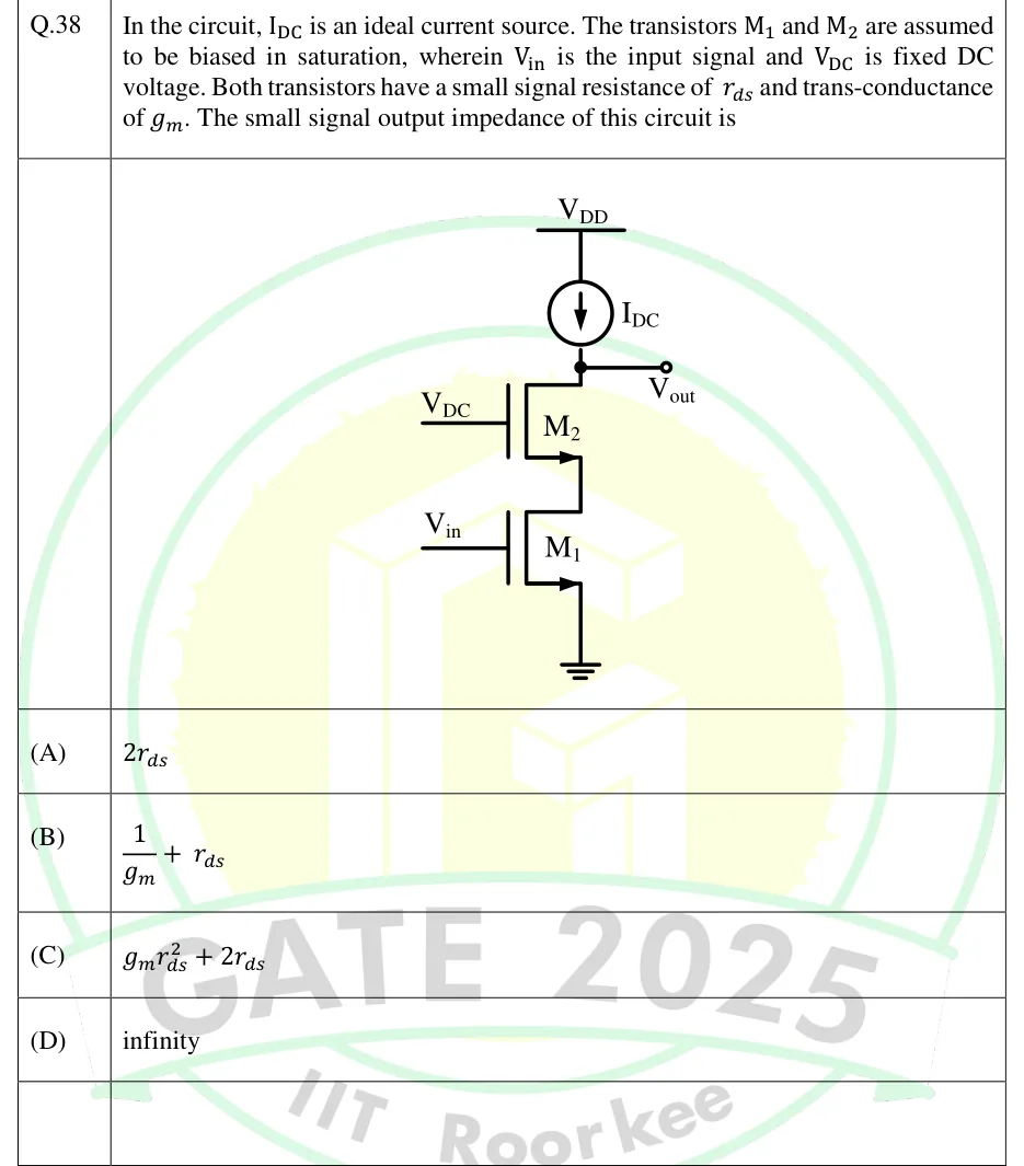
GATE 2025 EE question 38: NMOS cascode stage.Tap to open full size
Figure from the GATE 2025 EE paper. It is part of the question.
Figure description

NMOS cascode stage. From the V_DD rail an ideal current source I_DC (arrow pointing down) feeds a node that is brought out as the output terminal V_out. That node is the drain of NMOS M_2 (upper transistor), whose gate is at the fixed DC voltage V_DC. The source of M_2 (arrow on source) goes to the drain of NMOS M_1 (lower transistor), whose gate is driven by the input V_in. The source of M_1 is grounded. No resistors appear anywhere in the circuit.

  1. (A)

  2. (B)

  3. (C)

  4. (D)

    infinity

Answer and solution

ANSWER

The small-signal output impedance is , option (C).

Official answer: CSource: Official answer key, GATE 2025 EE (IIT Roorkee)

  1. Set up the small-signal circuit. To find the output impedance, set the input to zero. becomes AC ground. is a fixed DC voltage, so the gate of is also at AC ground. An ideal current source has infinite small-signal resistance, so it is an open circuit. What remains is the cascode –, seen from the drain of .

  2. Model. Both MOSFETs are in saturation. Each is modelled as a controlled source from drain to source, with in parallel with it. Body effect is neglected, because the question gives only and .

  3. Apply a test source. Drive a test voltage into the node. The current it delivers flows down through and then through to ground, since the source of connects only to the drain of .

  4. Lower device . Its gate and source are both at AC ground, so . Its controlled source is therefore dead and acts as a plain resistor . The whole of flows through it, so the voltage at the source of is .

  5. Upper device . With its gate at AC ground, . KCL at the drain of : the current entering the drain splits between the controlled source and , so

  6. Solve for . Multiply through by and collect terms: The resistance looking into the drain of is therefore .

  7. Combine with the current source. The ideal current source (infinite resistance) is in parallel with this at the output node, so This is option (C).

KEY IDEA

Looking into the drain of a MOSFET whose source has a resistance to ground gives . In a cascode, is the of the lower transistor, so . The ideal current-source load is an open circuit in parallel with this, so it leaves the result unchanged.

WATCH OUT FOR

Choosing (D) because the load is an ideal current source. The infinite resistance is in PARALLEL with the cascode at the output node, not in series, so it drops out and leaves the finite cascode resistance. Choosing (A) means treating as nothing more than and missing the boost that comes from its source being degenerated by . Choosing (B) means treating as a source follower or diode (), but here the output is taken at its drain.

From the GATE 2025 EE paper. Every question of this paper · Download the full paper · All 20 Amplifiers questions, with notes

More Amplifiers questions